Multi Channel DMA for PCI Express* Intel® FPGA IP Design Example User Guide
A newer version of this document is available. Customers should click here to go to the newest version.
3.3.1. Testbench Overview
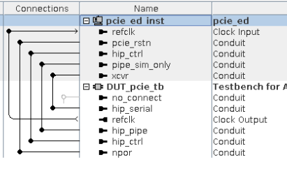
The design example, pcie_ed_inst, is generated with x16. The Intel FPGA BFM, DUT_pcie_tb, can support up to x8 link. The BFM supports the testbench simulation by down-training to x8 link. If you want to simulate x16 link, you can use a third-party BFM.
The testbench uses a Root Port driver module, altpcietb_bfm_rp_gen3_x8.sv ( Path: pcie_ed_tb/ip/pcie_ed_tb/DUT_pcie_tb_ip/altera_pcie_s10_tbed_191/sim ), to exercise the target memory and DMA channel in the Endpoint. This is the module that you can modify to vary the transactions sent to the example Endpoint design or your own design.
For more information about Intel FPGA BFM, refer to Intel Stratix 10 Avalon streaming and SR-IOV Interface for PCI Express Solutions User Guide (Section 9.3 Root Port BFM Overview).