External Memory Interfaces Intel® Agilex™ FPGA IP User Guide
A newer version of this document is available. Customers should click here to go to the newest version.
9.3.1. Address/Command Simulation Deck
The configuration has the following characteristics:
- Two pins within the 12-pin lane are driven with a differential clock pattern to map to the CK0 and CK0_N clock pairs. These pins are driven with a repeating clock pattern, phase-adjusted such that the rising/falling edge of CK0/CK0_N are centered within the valid data window.
- For DDR4, CK0/CK0_N map to pins 8/9 within the lane.
- For QDR4, CK0/CK0_N map to pins 4/5 within the lane.
- The symbol rate of the address/command pins matches the characteristics of the memory technology.
- For DDR4, the address/command channel is single-data-rate.
- For QDR4, the address/command channel is double-data-rate.
- One pin is designated as a victim pin, driven with a PRBS-10 pattern (repeated three times).
- For DDR4, pin 5 is designated as the victim pin.
- For QDR4, pin 8 is designated as the victim pin.
- The remaining pins are driven with the same aggressor PRBS-15 data pattern.
The structure of the address/command simulation deck is illustrated below.
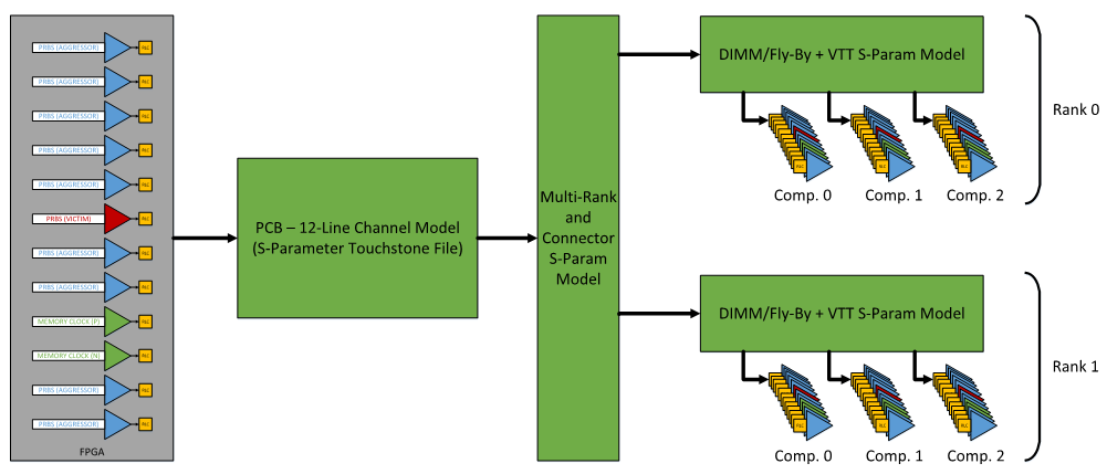
The simulation deck assumes a 12-line channel model; the purpose of each block is described in the sections below.
FPGA
At the far left of the above diagram, 12 FPGA IBIS models are instantiated and configured to match the IP-specified memory-clock and address/command electrical settings. The pattern generators are embedded within this sub-circuit and automatically configured via the IP-generated parameter file.
PCB — 12-Line Channel Model
This block connects to a 12-line (24-port plus ground) channel model that matches the signals implementing Lane 0 of the address/command bus for that interface. By default, this subcircuit instantiates 12 independent ideal 50-ohm transmission lines, which can be replaced by specifying the following options in the IP-generated parameter file:
| Parameter Name | Default Value | Description |
|---|---|---|
| USE_AC_PCB_EXTRACTION | False | Specifies if a 24-port Touchstone extraction is to be used in the Address/Command simulation. If set to true, then the AC_PCB_EXTRACTION_FILE parameter must specify a valid Touchstone file location. If set to false, ideal transmission line models are used. |
| AC_PCB_EXTRACTION_FILE | <empty> | Specifies the file name for the 24-port Touchstone extraction file (.s24p) that represents the address/command channel. The first 12 pins map to Lane 0, Pins 0 through 11 connected to the balls of the FPGA. The next 12 pins map to the far-end of the channel, which is either the memory balls (for direct point-to-point connections) or to the bifurcation point for a multi-rank topology. |
Multi-Rank and Connector Model
Use this block in cases where you want to do the following:
- Model the multi-rank topology of your interface to explore the effect of parameters such as DIMM spacing, channel loading, or component stacking.
- Model the effect of the DIMM connector by inserting a vendor-supplied simulation model.
This block is situated between the end of the address/command PCB extraction model and the start of the fly-by topology for each rank. If you don't specify an extraction model, then the default model of the block is as follows:
- For single rank DDR4 systems, the default model for this block is a direct pass-through.
- For dual-rank DDR4 systems, the default model for this block is to connect directly to rank 0, and insert 12 independent 50-ohm, 50ps transmission lines between rank 0 and rank 1 to model a slight delay difference between the two ranks.
- For quad-rank DDR4 systems, the default model for this block is to connect directly to ranks 0 and 1, and insert 12 independent 50-ohm, 50ps transmission lines between ranks 0/1 and ranks 2/3.
You can override this default behavior by specifying an S-Parameter model of your own, using the following options. (Note that the number of ports of the model should align with the IP-calculated value of the number of A/C ranks in the system, MEMAC_RANKS. A value of 1, 2 or 4 correspond to single, dual- or quad-rank systems and require 24, 36 or 60-port models, respectively.)
| Parameter Name | Default Value | Description |
|---|---|---|
| USE_AC_MULTIRANK_CONNECTOR_EXTRACTION | False | Specifies if a N-port Touchstone extraction is to be used in the address/command simulation to model the multi-rank bifurcation topology or the DIMM connector. If set to true, then the AC_MULTIRANK_CONNECTOR_EXTRACTION_FILE parameter must specify a valid Touchstone file location. If set to false, ideal transmission line models are used. |
| AC_MULTIRANK_CONNECTOR_EXTRACTION_FILE | <empty> | Specifies the file name for the N-port Touchstone extraction file (.sNp) that represents the address/command channel. The first 12 pins map to Lane 0, Pins 0 through 11 connected to the endpoint of the 12-line A/C channel model. The next 12 pins connect to the start of the A/C Fly-by topology for Rank 0. If MEMAC_RANKS is greater than 1, the next 12 pins connect to the address/command fly-by topology for Rank 1, and Rank 2 and Rank 3 for quad-rank systems. |
DIMM/Fly-By + VTT Model
This block models the fly-by topology of the address/command bus for a multi-component memory interface. You can use this file to adjust factors that can affect the signal integrity of the address/command interface, including the following:
- Component loading
- Component spacing
- Trace geometry/impedance between components
- Effect of using DDP components vs planar components
- Effect of placement/value of termination resistor network
- Effect of trace spacing on signal integrity
- Effect of vias, back-drilling, or placement of components on both sides of board
By default, this block generates MEMAC_COMP_PER_RANKS components in the fly-by chain. The first component is connected directly to the first 12 ports of the subcircuit. Subsequent components are connected to the previous component using 12 independent 50-ohm, 50ps ideal transmission lines. The final component in the flyby chain has each of its signals terminated to the VTT source via 50-ohm resistors. Note that the differential clock is AC-coupled to the VTT source through a 0.01uF capacitor.
You can override this default behavior by specifying an S-Parameter model of your own, using the following options. (Note that the number of ports of the model should align with the IP-calculated value of the number of A/C components in the system, MEMAC_COMP_PER_RANKS. The minimum number of ports for a value of 1 is 24 ports, increasing by 12 ports for every additional component in the flyby chain.
| Parameter Name | Default Value | Description |
|---|---|---|
| USE_AC_FLYBY_EXTRACTION | False | Specifies if an N-port Touchstone extraction is to be used in the address/command simulation to model the fly-by topology. If set to true, then the AC_FLYBY_EXTRACTION_FILE parameter must specify a valid Touchstone file location. If set to false, ideal transmission line models are used. |
| AC_FLYBY_EXTRACTION_FILE | <empty> | Specifies the file name for the N-port Touchstone extraction file (.sNp) that represents the address/command channel. The first 12 pins map to Lane 0, Pins 0 through 11 connected to the endpoint of the 12-line A/C multirank/connector model. The next 12 pins connect to the first component of the address/command Fly-by topology. If MEMAC_COMP_PER_RANKS is greater than 1, the next 12 pins connect to each additional component in the chain up to a maximum of 9 components (a 12-port model). |