External Memory Interfaces Intel® Agilex™ FPGA IP User Guide
A newer version of this document is available. Customers should click here to go to the newest version.
3.6.1. Restrictions on I/O Bank Usage for Intel® Agilex™ EMIF IP with HPS
The restrictions on I/O bank usage result from the Intel® Agilex™ HPS having hard-wired connections to the EMIF circuits in the I/O banks closest to the HPS. For any given EMIF configuration, the pin-out of the EMIF-to-HPS interface is fixed.
The following diagram illustrates the use of I/O banks and lanes for various EMIF-HPS data widths:
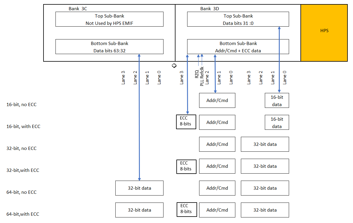
The HPS EMIF uses the closest located external memory interfaces I/O banks to connect to SDRAM. This arrangement of HPS EMIF address and command sub-banks relative to the data sub-banks is not supported for fabric EMIF in the current version of the Intel® Quartus® Prime Design Suite.
The following diagram illustrates restrictions on I/O pin usage. Refer to the text following the diagram for a detailed explanation of these restrictions.
The HPS EMIF IP must be used whenever the HPS is active. Thus, you should be aware that enabling the HPS necessarily means that an EMIF must be placed at this location in order to implement an FPGA design.
If there is an HPS EMIF in a system, the unused HPS EMIF pins can be used as FPGA general purpose I/O, with the following restrictions:
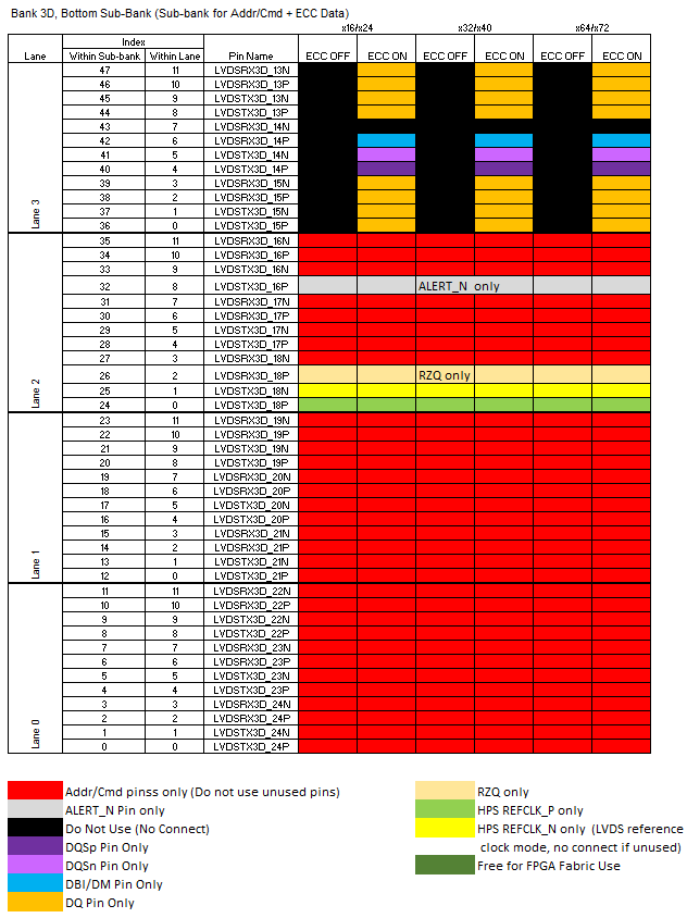
- Bank 3D, Bottom Sub-bank (Sub-bank for Address/Command + ECC Data):
- Lane 3 is used for data bits only when ECC mode is active. Whether ECC is active or not, you must not put general purpose I/Os in this lane.
- Lanes 2, 1, and 0 are used for SDRAM address and command. Unused pins in these lanes must not be used by the FPGA fabric.
- ALERT_N pin must be placed at pin index 8, lane 2. There is no flexibility on this,
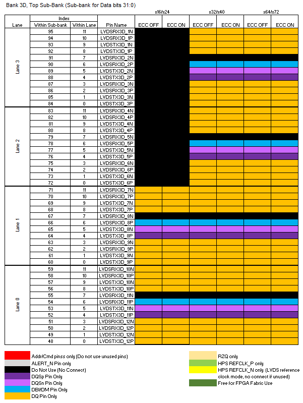
- Bank 3D, Top Sub-bank (Sub-bank for data bits 31:0) :
- Lanes 3, 2, 1, and 0 are used for data bits.
- With 32-bit data widths, unused pins in this bank must not be used by the FPGA fabric.
- With 16-bit data widths, lanes 0 and 1 are used as data lanes. Unused pins in lane 0 and lane 1 must not be used by FPGA fabric. Unused pins in lanes 2 and 3 must not be used by the FPGA fabric, even though lanes 2 and 3 are not used by HPS EMIF.
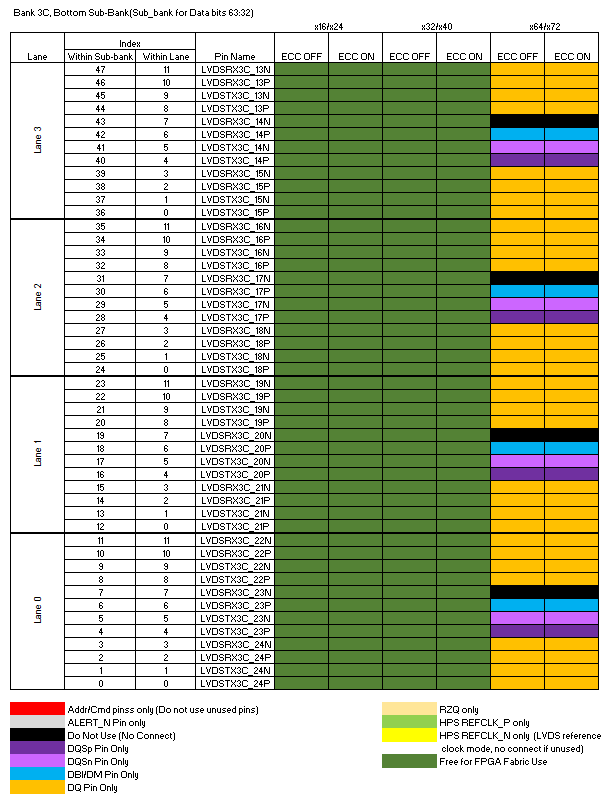
- Bank 3C, Bottom Sub-bank (Sub-bank for Data bits 63:32)
- With 64-bit data widths, lanes 3, 2, 1, and 0 are used for data bits [63:32]. Unused pins in these lanes must not be used by the FPGA fabric.
- With 32-bit data widths, the entire bottom sub-bank can be used by the FPGA fabric. There are no restrictions.
- Bank 3C, Top Sub-bank
- Not used by HPS EMIF. Unused pins in this bank can be used by FPGA fabric when the bottom sub-bank in 3C is not used for 64-bit HPS EMIF.
- The following restrictions apply on the top sub-bank when the bottom sub-bank in 3C is used for 64-bit HPS EMIF:
- This sub-bank can be used to form a larger non-HPS EMIF, but you cannot place an address and command bank in this sub-bank.
- 1.5V true differential signaling is not supported.
- I/O PLL reconfiguration is not supported.
By default, the Intel® Agilex™ External Memory Interface for HPS IP core together with the Intel® Quartus® Prime Fitter automatically implements a starting point placement which you may need to modify. You must adhere to the following requirements, which are specific to HPS EMIF:
- Within a single data lane (which implements a single x8 DQS group):
- DQ pins must use pins at indices 0, 1, 2, 3, 8, 9, 10, 11. You may swap the locations between the DQ bits (that is, you may swap location of DQ[0] and DQ[3]) so long as the resulting pin-out uses pins at these indices only.
- DM/DBI pin must use pin at index 6. There is no flexibility.
- DQS and DQS# must use pins at index 4 and 5, respectively. There is no flexibility.
- Pin index 7 must have no fabric usage and cannot implement general purpose I/Os.
- In all cases the DQS groups can be swapped around the I/O banks shown. There is no requirement for the ECC DQS group to be placed in the bottom sub-bank in bank 3D.
- In the bottom sub-bank in bank 3D (sub-bank for address and command + ECC data):
- You must not change placement of the address and command pins from the default.
- Place the alert# pin in lane 2, pin index 8.
- Place the PLL reference clock in this sub-bank. Failure to place the PLL reference clock in this sub-bank causes device configuration problems. The PLL reference clock must be running at the correct frequency before device configuration occurs.
- Place the RZQ pin in this sub-bank. Failure to place the RZQ pin in this sub-bank causes Fitter or device configuration problems.
- To override the default generated pin assignments, comment out the relevant HPS_LOCATION assignments in the .qip file, and add your own location assignments (using set_location_assignment) in the .qsf file.