External Memory Interfaces Intel® Agilex™ FPGA IP User Guide
A newer version of this document is available. Customers should click here to go to the newest version.
7.4.2. Reference Stackup
It is important to understand that trace geometry such as width, thickness, and edge-to-edge spacing, and the distance to reference planes, all impact trace impedance and crosstalk levels.
| Layer | Type | Thickness |
|---|---|---|
| SM TOP | 0.5 | |
| L1 | signal | 1.8 |
| D1 | prepreg | 2.7 |
| L2 | gnd/power | 1.2 |
| D2 | core | 4.0 |
| L3 | signal | 1.2 |
| D3 | prepreg | 6.3 |
| L4 | gnd/power | 1.2 |
| D4 | core | 4.0 |
| L5 | signal | 1.2 |
| D5 | prepreg | 6.3 |
| L6 | gnd/power | 1.2 |
| D6 | core | 4.0 |
| L7 | signal | 1.2 |
| D7 | prepreg | 6.3 |
| L8 | gnd | 1.2 |
| D8 | core | 4 |
| Power | 1.2 | |
| prepreg | 6.3 | |
| power | 1.2 | |
| core | 4 | |
| gnd | 1.2 | |
| prepreg | 6.3 | |
| power | 1.2 | |
| core | 4 | |
| L9 | gnd | 1.2 |
| D9 | prepreg | 6.3 |
| L10 | signal | 1.2 |
| D10 | core | 4.0 |
| L11 | gnd/power | 1.2 |
| D11 | prepreg | 6.3 |
| L12 | signal | 1.2 |
| D12 | core | 4.0 |
| L13 | gnd/power | 1.2 |
| D13 | prepreg | 6.3 |
| L14 | signal | 1.2 |
| D14 | core | 4.0 |
| L15 | gnd/power | 1.2 |
| D15 | prepreg | 2.7 |
| L16 | signal | 1.8 |
| SM BOT | 0.5 | |
| Total | 120.1 |

The reference stackup height is selected to be 120 mil to cover maximum signal via coupling (110mil) in simulation while extracting EMIF design guideline. Intel® recommends that board designers do not exceed 110mil signal via coupling (stripline routing on inner layers) in the EMIF layout PCB design.
If the PCB stackup exceeds 120 mil in height, Intel® recommends routing EMIF signals on upper layers, not to exceed more than 110 mil of signal via coupling.
The reference stackup materials in the above figure are selected as FR4, to represent worse-case signal loss in design phase simulation. In case of low-loss materials, the maximum end-to-end routing length shall be larger than the recommended end-to-end routing length in the design guidelines; however, you must perform time-domain channel simulation to ensure that timing requirements are met.
The Intel® Agilex™ family pin floorplan is a HEX pattern with 1mm pitch. The following figure shows an example of routing for an IO12 (one-byte data) on PCB within FPGA fan-out region.
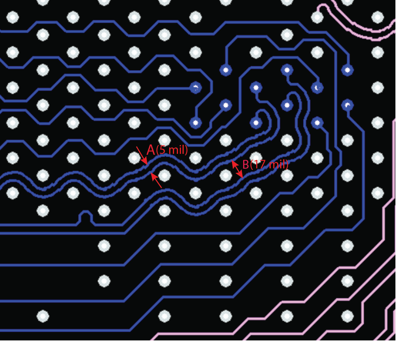
The following general notes apply to the EMIF routing guidelines for QDR-IV topologies:
- All spacing requirements are the minimum requirement to be met on PCB in EMIF routing guideline table.
- Breakout (BO1/BO2) spacings have two different values in guideline tables. The first value represents minimum spacing between two signals routed as a pair (tightly coupled signals); this value is marked as A (5 mil) in the above figure. The second value represents minimum spacing between two pairs, and is marked as B (17 mil) in the above figure.
- Main route (M) spacings have both value in mil and formula. In formula, h represents the trace-to-nearest-reference-plane height or distance. In cases using a stackup different than the reference stackup, board designers shall use formula to calculate the correct spacing requirements.
- There is no differential impedance target for CLK nor QK/DK. Board designers shall follow single-ended impedance target and keep the signals within the pair closely coupled, within 3-4 mil spacing. For information on QK/DK and CLK/CLKB, refer to Skew Matching Guidelines for QDR-IV Configurations .
- In guideline tables, SL stands for stripline routing recommendation and US stands for upper surface (Microstrip) routing recommendation.
- The trace width value/geometry in guideline tables stands for trace designed for target impedance based on the reference stackup. This trace geometry shall be designed based on actual stackup and target impedance in guideline table.
- In guideline tables, BO1 and BO2 represent fan-out routing lengths. M stands for out of fan-out (PCB main) routing lengths