High Bandwidth Memory (HBM2) Interface FPGA IP User Guide
ID
683189
Date
3/29/2024
Public
1. About the High Bandwidth Memory (HBM2) Interface Intel® FPGA IP
2. Introduction to High Bandwidth Memory
3. Stratix® 10 HBM2 Architecture
4. Creating and Parameterizing the High Bandwidth Memory (HBM2) Interface Intel® FPGA IP
5. Simulating the High Bandwidth Memory (HBM2) Interface Intel® FPGA IP
6. High Bandwidth Memory (HBM2) Interface Intel® FPGA IP Interface
7. High Bandwidth Memory (HBM2) Interface Intel® FPGA IP Controller Performance
8. High Bandwidth Memory (HBM2) Interface Intel® FPGA IP User Guide Archives
9. Document Revision History for High Bandwidth Memory (HBM2) Interface FPGA IP User Guide
4.2.1. General Parameters for High Bandwidth Memory (HBM2) Interface Intel® FPGA IP
4.2.2. FPGA I/O Parameters for High Bandwidth Memory (HBM2) Interface Intel® FPGA IP
4.2.3. Controller Parameters for High Bandwidth Memory (HBM2) Interface Intel® FPGA IP
4.2.4. Diagnostic Parameters for High Bandwidth Memory (HBM2) Interface Intel® FPGA IP
4.2.5. Example Designs Parameters for High Bandwidth Memory (HBM2) Interface Intel® FPGA IP
4.2.6. Register Map IP-XACT Support for HBM2 IP
5.1. High Bandwidth Memory (HBM2) Interface Intel® FPGA IP Example Design
5.2. Simulating High Bandwidth Memory (HBM2) Interface Intel® FPGA IP with ModelSim* and Questa*
5.3. Simulating High Bandwidth Memory (HBM2) Interface Intel® FPGA IP with Synopsys VCS*
5.4. Simulating High Bandwidth Memory (HBM2) Interface Intel® FPGA IP with Riviera-PRO*
5.5. Simulating High Bandwidth Memory (HBM2) Interface Intel® FPGA IP with Cadence Xcelium* Parallel Simulator
5.6. Simulating High Bandwidth Memory (HBM2) Interface Intel® FPGA IP for High Efficiency
5.7. Simulating High Bandwidth Memory (HBM2) Interface IP Instantiated in Your Project
6.1. High Bandwidth Memory (HBM2) Interface Intel® FPGA IP High Level Block Diagram
6.2. High Bandwidth Memory (HBM2) Interface Intel® FPGA IP Controller Interface Signals
6.3. User AXI Interface Timing
6.4. User APB Interface Timing
6.5. User-controlled Accesses to the HBM2 Controller
6.6. Soft AXI Switch
7.1. High Bandwidth Memory (HBM2) DRAM Bandwidth
7.2. High Bandwidth Memory (HBM2) Interface Intel® FPGA IP HBM2 IP Efficiency
7.3. High Bandwidth Memory (HBM2) Interface Intel® FPGA IP Latency
7.4. High Bandwidth Memory (HBM2) Interface Intel® FPGA IP Timing
7.5. High Bandwidth Memory (HBM2) Interface Intel® FPGA IP DRAM Temperature Readout
2.1. HBM2 in Intel® Stratix® 10 Devices
Stratix® 10 devices incorporate a high-performance FPGA fabric along with a HBM2 DRAM in a single package. Stratix® 10 devices support up to a maximum of two HBM2 interfaces.
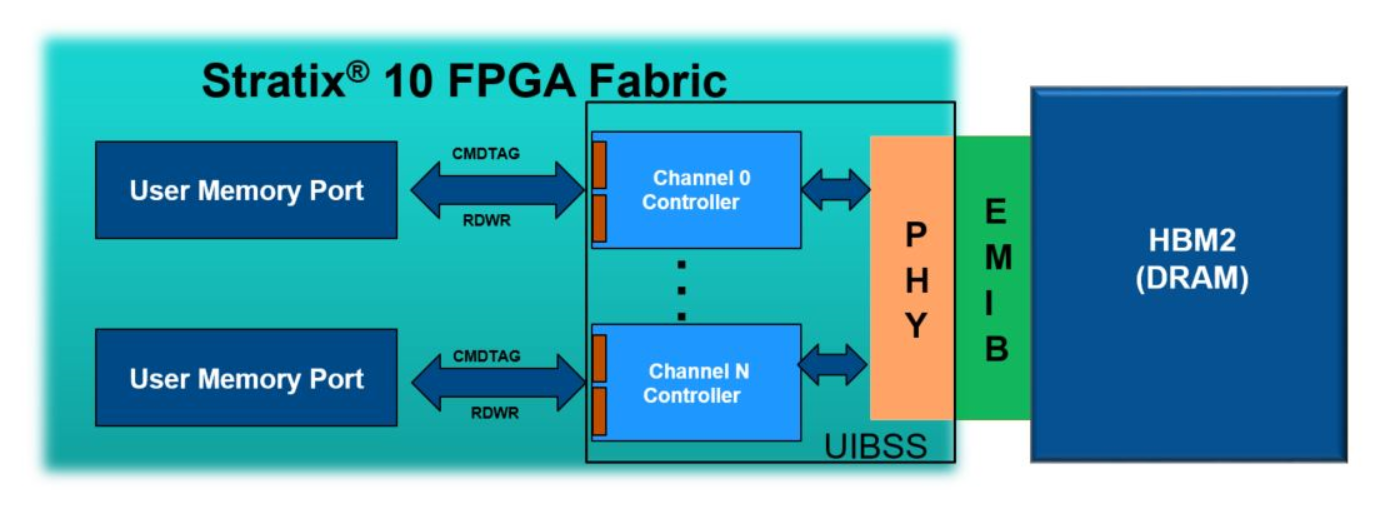
Stratix® 10 devices incorporate Intel’s Embedded Multi-Die Interconnect Bridge (EMIB) technology to implement a silicon bridge between HBM2 DRAM memory and the Universal Interface Block Subsystem (UIBSS), which contains the HBM2 controller (HBMC), physical-layer interface (PHY), and I/O ports to interface to the HBM2 stack.
As illustrated below, each Stratix® 10 device contains a single universal interface bus per HBM2 interface, supporting 8 independent channels.
The user interface to the HBM2 controller is maintained through the AXI4 protocol. Sixteen AXI interfaces are available in the user interface from each HBM2 controller, with one AXI interface available per HBM2 Pseudo Channel. HBM2 DRAM density of 4GB and 8GB are supported.
Figure 1. Stratix® 10 Device with UIB, EMIB, and HBM2 DRAM