Intel® Quartus® Prime Pro Edition User Guide: Power Analysis and Optimization
A newer version of this document is available. Customers should click here to go to the newest version.
1.4. Viewing Power Analysis Reports
Summary
Following successful power analysis, click the Power Analyzer pulldown in the Table of Contents of the Compilation Report, to view the Power Analysis section of the report.
The Power Analysis reports contains the following sections:
The Summary section of the report shows the estimated total thermal power consumption of your design. This includes dynamic, static, and I/O thermal power consumption. The I/O thermal power includes the total I/O power drawn from the VCCIO and VCCPD power supplies and the power drawn from VCCINT in the I/O subsystem including I/O buffers and I/O registers. The report also includes a confidence metric that reflects the overall quality of the data sources for the signal activities. For example, a Low power estimation confidence value reflects that you have provided insufficient toggle rate data, or most of the signal activity information used for power estimation is from default or vectorless estimation settings. For more information about the input data, refer to the Power Analyzer Confidence Metric report.
Power Savings Summary
Lists any savings (in mW) and the type of savings method, such as SmartVID Power Savings.
Parallel Compilation
When you enable parallel compilation, the Parallel Compilation report list the number of processors you use during Power Analysis
Settings
The Settings section of the report shows the Power Analyzer settings information of your design, including the default input toggle rates, operating conditions, and other relevant setting information.
Simulation Files Read
The Simulation Files Read section of the report lists the simulation output file that the .vcd used for power estimation. This section also includes the file ID, file type, entity, VCD start time, VCD end time, the unknown percentage, and the toggle percentage. The unknown percentage indicates the portion of the design module unused by the simulation vectors.
Operating Conditions Used
The Operating Conditions Used section of the report shows device characteristics, voltages, temperature, and cooling solution, if any, during the power estimation. This section also shows the entered junction temperature or auto-computed junction temperature during the power analysis.
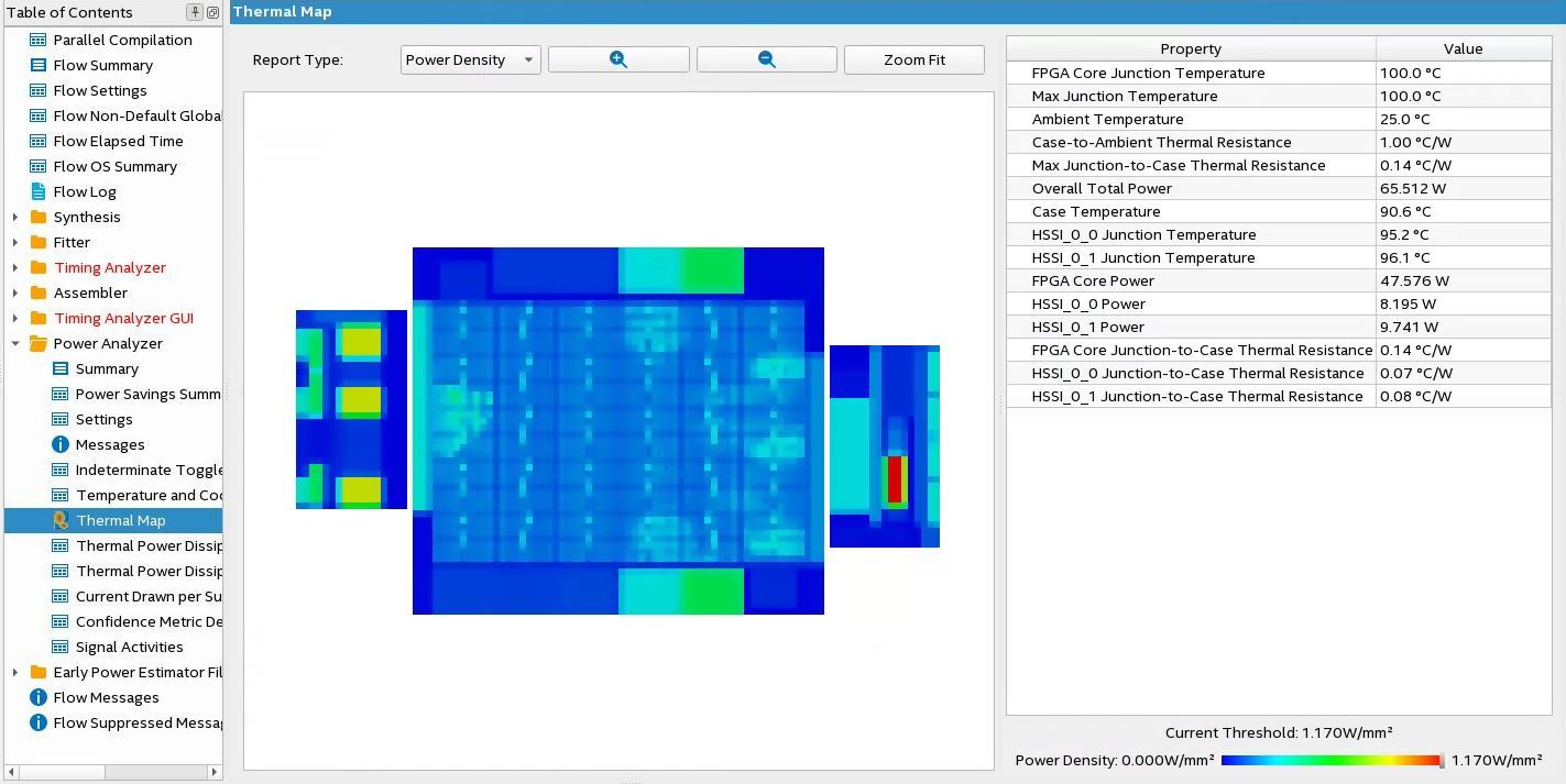
Thermal Map Visualization
For Intel® Agilex™ FPGA designs, the Power Analyzer provides a visualization of the expected thermal distribution on the core die and the transceiver dies. This data is available when you run the Power Analyzer on your compiled Intel® Agilex™ FPGA design. After you run the Power Analyzer, select the Thermal Map section in the Power Analyzer report. You can set the threshold temperature you want to use, which is useful if you are making any what-if analyses based on your thermal design. You can adjust the threshold temperature in increments of 5°C, between the ambient temperature (or 50°C, whichever is lower), and an upper limit of 100°C.
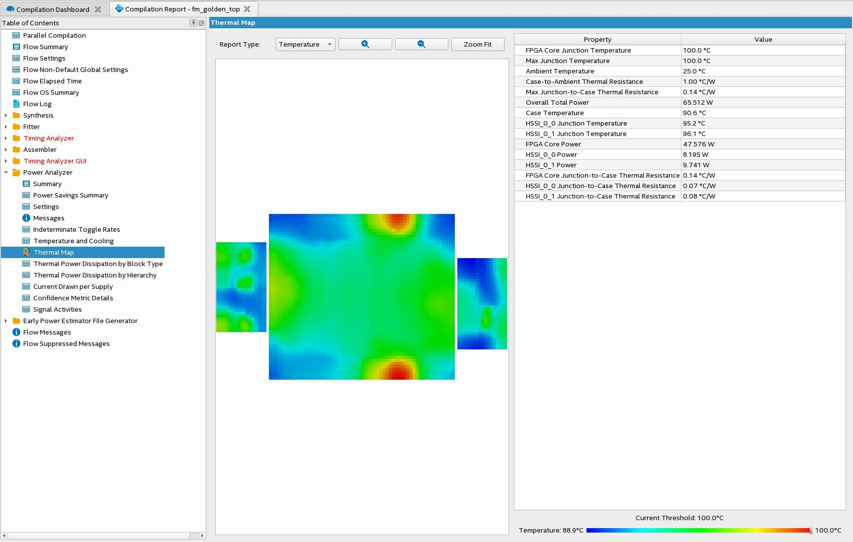
Knowing the locations of hot spots in your design can help you make modifications as necessary for proper operation of the system.
The thermal map report can show two different views—a temperature view and a power density view. You can choose the view from a pulldown selection in the GUI, when you open the thermal map in the Power Analyzer.
Thermal Power Dissipated by Block
The Thermal Power Dissipated by Block section of the report shows estimated thermal dynamic power and thermal static power consumption categorized by atoms. This information provides you with estimated power consumption for each atom in your design.
By default, this section does not contain any data, but you can turn on the report with the Write power dissipation by block to report file option on the Power Analyzer Settings page.
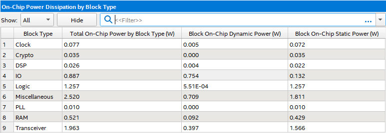
On-Chip Power Dissipation by Block Type
The On-Chip Power Dissipation by Block Type section of the report shows the estimated total on-chip power consumption by block type, and estimated on-chip dynamic power and estimated on-chip static power, by block type.
On-Chip Power Dissipation by Hierarchy
This On-Chip Power Dissipation by Hierarchy section of the report shows estimated total on-chip power consumption by hierarchy node, and both the cumulative and current-hierarchy-level dynamic, static, and routing power consumptions. This information is useful when locating modules with high power consumption in your design. (Available for Intel® Agilex™ devices.)
Core Dynamic Thermal Power Dissipation by Clock Domain
The Core Dynamic Thermal Power Dissipation by Clock Domain section of the report shows the estimated total core dynamic power dissipation by each clock domain, which provides designs with estimated power consumption for each clock domain in the design. If the clock frequency for a domain is unspecified by a constraint, the clock frequency is listed as “unspecified.” For all the combinational logic, the clock domain is listed as no clock with zero MHz.
Current Drawn per Supply
The Current Drawn per Supply section of the report lists the current drawn from each voltage supply. The VCCIO and VCCPD voltage supplies are further categorized by I/O bank and by voltage. This section also lists the minimum safe power supply size (current supply ability) for each supply voltage. Minimum current requirement can be higher than user mode current requirement in cases in which the supply has a specific power up current requirement that goes beyond user mode requirement.
The I/O thermal power dissipation on the summary page does not correlate directly to the power drawn from the VCCIO and VCCPD voltage supplies listed in this report. This is because the I/O thermal power dissipation value also includes portions of the VCCINT power, such as the I/O element (IOE) registers, which are modeled as I/O power, but do not draw from the VCCIO and VCCPD supplies.
The reported current drawn from the I/O Voltage Supplies (ICCIO and ICCPD) as reported in the Power Analyzer report includes any current drawn through the I/O into off-chip termination resistors. This can result in ICCIO and ICCPD values that are higher than the reported I/O thermal power, because this off-chip current dissipates as heat elsewhere and does not factor in the calculation of device temperature. Therefore, total I/O thermal power does not equal the sum of current drawn from each VCCIO and VCCPD supply multiplied by VCCIO and VCCPD voltage.
For SoC devices, there is no standalone ICC_AUX_SHARED current drawn information. The ICC_AUX_SHARED is reported together with ICC_AUX.
Confidence Metric Details
The Confidence Metric is defined in terms of the total weight of signal activity data sources for both combinational and registered signals. Each signal has two data sources allocated to it; a toggle rate source and a static probability source.
The Confidence Metric Details section also indicates the quality of the signal toggle rate data to compute a power estimate. The confidence metric is low if the signal toggle rate data comes from poor predictors of real signal toggle rates in the device during an operation. Toggle rate data that comes from simulation, user-entered assignments on specific signals or entities are reliable. Toggle rate data from default toggle rates (for example, 12.5% of the clock period) or vectorless estimation are relatively inaccurate. This section gives an overall confidence rating in the toggle rate data, from low to high. This section also summarizes how many pins, registers, and combinational nodes obtained their toggle rates from each of simulation, user entry, vectorless estimation, or default toggle rate estimations. This detailed information helps you understand how to increase the confidence metric, letting you determine your own confidence in the toggle rate data.
Signal Activities
The Signal Activities section lists toggle rates and static probabilities assumed by power analysis for all signals with fan-out and pins. This section also lists the signal type (pin, registered, or combinational) and the data source for the toggle rate and static probability. By default, this section does not contain any data, but you can turn on the report with the Write signal activities to report file option on the Power Analyzer Settings page.
Intel recommends that you keep the Write signal activities to report file option turned off for a large design because of the large number of signals present. You can use the Assignment Editor to specify that activities for individual nodes or entities are reported by assigning an on value to those nodes for the Power Report Signal Activities assignment.
Messages
The Messages section lists the messages that the Intel® Quartus® Prime software generates during the analysis.