AN 916: JESD204C Intel® FPGA IP and ADI AD9081/AD9082 MxFE* Interoperability Report for Intel® Stratix® 10 E-Tile Devices
ID
683157
Date
6/22/2020
Public
1.1. Hardware Requirements
1.2. Hardware Setup
1.3. JESD204C Intel® FPGA IP and ADC Hardware Checkout
1.4. JESD204C Intel® FPGA IP and DAC Hardware Checkout
1.5. Document Revision History for AN 916: JESD204C Intel® FPGA IP and ADI AD9081/AD9082 MxFE* Interoperability Report for Intel® Stratix® 10 E-Tile Devices
1.6. Appendix
1.3.3. ADC Test Results
The following table contains the possible results and their definition.
| Result | Definition |
|---|---|
| PASS | The device under test (DUT) was observed to exhibit conformant behavior. |
| PASS with comments | The DUT was observed to exhibit conformant behavior. However, an additional explanation of the situation is included (example: due to time limitations, only a portion of the testing was performed). |
| FAIL | The DUT was observed to exhibit non-conformant behavior. |
| Warning | The DUT was observed to exhibit behavior that is not recommended. |
| Refer to comments | From the observations, a valid pass or fail could not be determined. An additional explanation of the situation is included. |
The following table shows the results for test cases SHA.1, SHA.2, EMBA.1, EMBA.2, EMBA.3, and RXTL.1 with subclass 0, and FCLK_MULP = 2.
| Test No. | L | M | F | E | Lane Rate (Mbps) | ADC Rate (Msps) | Link Clock (MHz) | Result |
|---|---|---|---|---|---|---|---|---|
| 1 | 8 | 8 | 2 | 1 | 24750 | 3000 | 187.5 | PASS |
The following figure shows the Signal Tap waveform of the ramp pattern data received at output of FPGA receiver transport layer.
Figure 4. Ramp Data Pattern Diagram
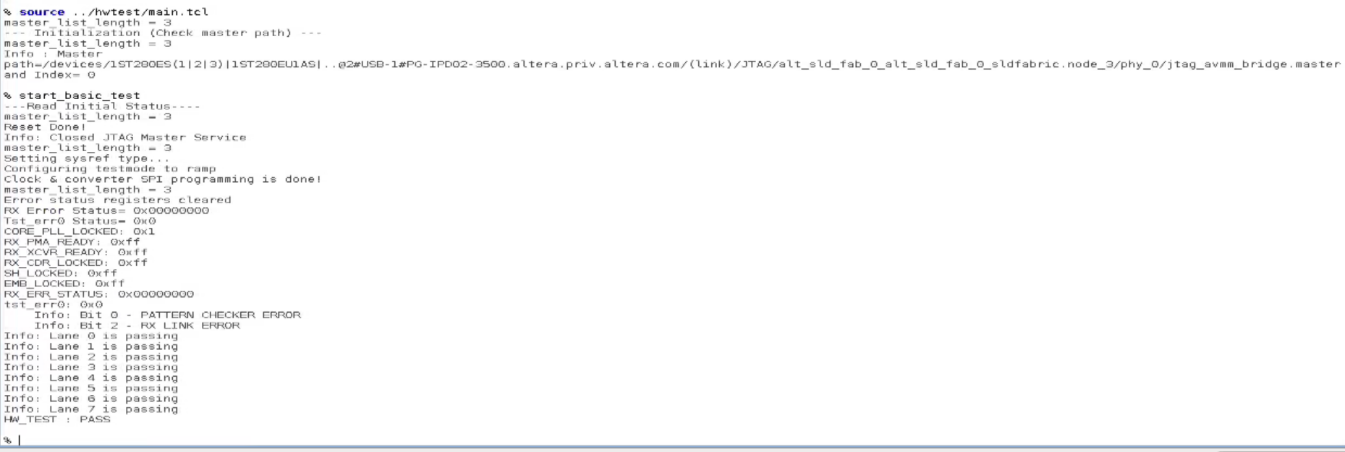
The following figure shows the result of the ramp pattern checker at output data of FPGA receiver transport layer.
Figure 5. Ramp Pattern Checker Result