GTS AXI Multichannel DMA IP for PCI Express* User Guide
5.1.4. AXI-MM BAM EP Memory Design Example
This design example enables the Bursting Master AXI-MM Manager interface, which bypasses the DMA path. This allows your application to perform bursting read/write operations with the on-chip memory in Bursting Master user mode.
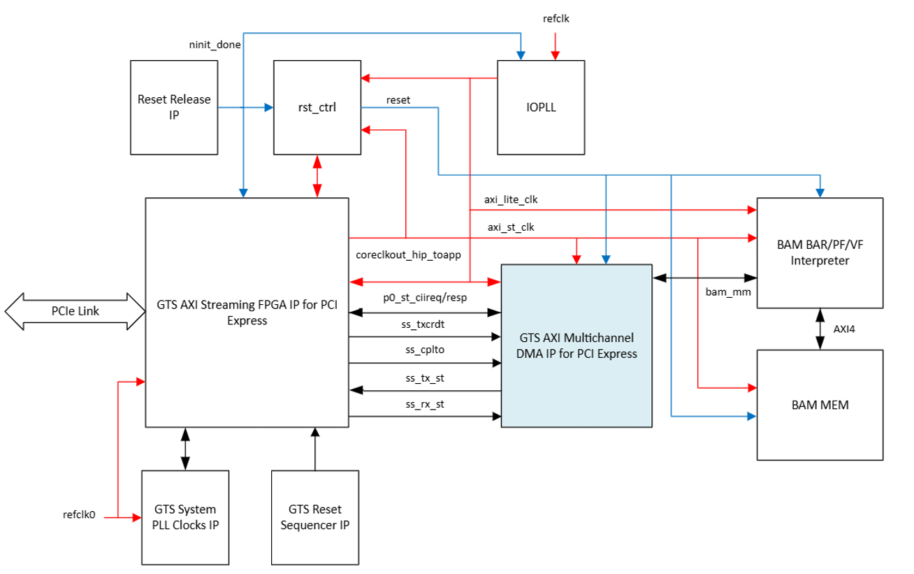
The AXI-MM BAM EP Memory design example includes the following components:
| Design Components | Descriptions |
|---|---|
| GTS AXI Streaming FPGA IP for PCI Express | Incorporate PCI Express (PCIe*) into your design utilizing an advanced PCIe hardened protocol stack, which encompasses the transaction, data link, and physical layers. It also includes optional components like Single Root I/O Virtualization (SR-IOV) for virtualization applications that demand high-bandwidth data transfer to and from the host memory. This component converts the PCIe serial link transfer to the AXI Stream interface and directs the TLP data received to the GTS AXI Multichannel DMA IP. |
| GTS AXI Multichannel DMA IP for PCI Express | Facilitates efficient data transfer between the local FPGA and the host through multiple DMA channels over the PCIe link. Each DMA channel comprises a host-to-device (H2D) and a device-to-host (D2H) queue pair, operating on descriptor-based queues established by the driver software for data transfer. It is engineered to support standalone Endpoint or Rootport functionality, offering AXI-S and AXI-MM interfaces to the user logic. |
| GTS System PLL Clocks IP | This IP is required for the PCIe interface implementation on Agilex™ 5 devices to configure the reference clock for the System PLL and provides the clock signal for p<n>_i_syspll_c0_clk of the GTS AXI Streaming IP.
Note: For more information, refer to the Implementing the GTS System PLL Clocks IP section in the GTS Transceiver PHY User Guide.
|
| GTS Reset Sequencer IP | This IP must be instantiated for each Agilex™ 5 FPGA side that uses transceivers for simulation and proper device operation. It provides the PMA Control Unit clock to the i_flux_clk clock of the GTS AXI Streaming IP.
Note: For more information, refer to the Implementing the GTS Reset Sequencer IP section in the GTS Transceiver PHY User Guide.
|
| Reset Release IP | This IP holds a control circuit in reset until the device has fully entered user mode. The FPGA asserts the INIT_DONE output to signal that the device is in user mode. It is required when using the GTS AXI Streaming IP.
Note: For more information on the Reset Release IP, refer to the Device Configuration User Guide: Agilex™ 5 FPGAs and SoCs.
|
| BAM Interface BAR/PF/VF Interpreter for MCDMA | This module interprets the BAM address mapping to decode the physical function number, virtual function number and address of the incoming packet. |
| BAM MEM | On-Chip Memory IP for BAM bursting read/write operations. |
| rst_ctrl_0 | This module handles the reset and handshake signals of the GTS AXI Streaming IP for graceful entry and exit for each of the resets (cold, warm, etc.) especially when initiated by the host system. |
| IOPLL FPGA IP | This IP is required to configure the settings of the Agilex™ 5 I/O PLL to provide a 100MHz clock signal for the AXI-Lite/MM interface in the design. |