GTS AXI Multichannel DMA IP for PCI Express* User Guide
ID
847470
Date
8/25/2025
Public
1. Overview
2. Quick Start Guide
3. Configuring and Generating the GTS AXI Multichannel DMA IP for PCI Express
4. Integrating the IP With Your Application
5. Simulating the IP
6. Validating the IP
7. Known Issues
A. Functional Description
B. Software Programming Model
C. Registers
D. Document Revision History for the GTS AXI Multichannel DMA IP for PCI Express*
2.1.1. Downloading and Installing Quartus® Prime Software
2.1.2. Configuring and Generating the GTS AXI Multichannel DMA IP for PCI Express
2.1.3. Configuring and Generating the GTS AXI Streaming IP for PCI Express
2.1.4. Configuring and Generating the GTS System PLL Clocks IP
2.1.5. Configuring and Generating the GTS Reset Sequencer IP
2.1.6. Configuring and Generating the Reset Release IP
2.1.7. Instantiating and Connecting the IP Interfaces
2.1.8. Simulate, Compile and Validate the Design on Hardware
4.4.1. PCIe AXI-Stream TX Interface (ss_tx_st)
4.4.2. PCIe AXI-Stream RX Interface (ss_rx_st)
4.4.3. Control and Status Register Interface (ss_csr_lite)
4.4.4. Transmit Flow Control Credit Interface (ss_txcrdt)
4.4.5. Configuration Intercept Interface (CII)
4.4.6. Completion Timeout Interface (ss_cplto)
4.4.7. Function Level Reset (FLR) Interface
4.4.8. Control Shadow Interface (ss_ctrlshadow)
4.4.9. Error Interface
4.5.1. H2D AXI-Stream Manager (h2d_st_initatr)
4.5.2. D2H AXI-Stream Subordinate (d2h_st_respndr)
4.5.3. H2D/D2H AXI-MM Manager (dma_mm_initatr)
4.5.4. BAM AXI-MM Manager (bam_mm_initatr)
4.5.5. BAS AXI-MM Subordinate (bas_mm_respndr)
4.5.6. PIO AXI-Lite Manager (pio_lite_initiatr)
4.5.7. HIP Reconfiguration AXI-Lite Subordinate (user_csr_lite)
4.5.8. User Event MSI-X (user_msix)
4.5.9. User Event MSI (user_msi)
4.5.10. User Function Level Reset (user_flr)
4.5.11. User Configuration Intercept Interface
4.5.12. Configuration Slave (cs_lite_respndr)
A.1.1.1. H2D Data Mover
A.1.1.2. D2H Data Mover
A.1.1.3. Descriptors
A.1.1.4. AXI4-Lite PIO Manager
A.1.1.5. AXI-MM Write (H2D) and Read (D2H) Manager
A.1.1.6. AXI-Stream Manager (H2D) and Subordinate (D2H)
A.1.1.7. User MSI-X
A.1.1.8. User Function Level Reset (FLR)
A.1.1.9. Control and Status Registers
B.1.6.1. ifc_api_start
B.1.6.2. ifc_mcdma_port_by_name
B.1.6.3. ifc_qdma_device_get
B.1.6.4. ifc_num_channels_get
B.1.6.5. ifc_qdma_channel_get
B.1.6.6. ifc_qdma_acquire_channels
B.1.6.7. ifc_qdma_release_all_channels
B.1.6.8. ifc_qdma_device_put
B.1.6.9. ifc_qdma_channel_put
B.1.6.10. ifc_qdma_completion_poll
B.1.6.11. ifc_qdma_request_start
B.1.6.12. ifc_qdma_request_prepare
B.1.6.13. ifc_qdma_descq_queue_batch_load
B.1.6.14. ifc_qdma_request_submit
B.1.6.15. ifc_qdma_pio_read32
B.1.6.16. ifc_qdma_pio_write32
B.1.6.17. ifc_qdma_pio_read64
B.1.6.18. ifc_qdma_pio_write64
B.1.6.19. ifc_qdma_pio_read128
B.1.6.20. ifc_qdma_pio_write128
B.1.6.21. ifc_qdma_pio_read256
B.1.6.22. ifc_qdma_pio_write256
B.1.6.23. ifc_request_malloc
B.1.6.24. ifc_request_free
B.1.6.25. ifc_app_stop
B.1.6.26. ifc_qdma_poll_init
B.1.6.27. ifc_qdma_poll_add
B.1.6.28. ifc_qdma_poll_wait
B.1.6.29. ifc_mcdma_port_by_name
3.4. Generating the Design Example
In the Quartus® Prime Pro Edition software, you can generate a design example for the GTS AXI Multichannel DMA IP for PCI Express.
Figure 23. Design Example Generation
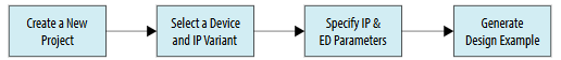
Following is the procedure to generate a design example:
- In the Quartus® Prime Pro Edition software, create a new project by clicking File → New Project Wizard. Click Next.
- Select Empty Project type and specify the Directory, Name, and Top-Level Entity. Click Next.
- Specify the Family, Device & Board Settings as follows:
- Select Family: Agilex™ 5 (E-Series/D-Series).
- Select Target device: A5ED065BB32AE4SR0.
Note: The device used for the Quartus® Prime-generated design example matches the device used in the target FPGA development kit board and may not be the same as the target device selected here.
- Click Finish.
- Select from Tools → IP Catalog to open the IP Catalog.
- Select GTS AXI Multichannel DMA IP for PCI Express (Library → Interface Protocols → PCI Express → GTS AXI Multichannel DMA IP for PCI Express) and then click Add.
- In the New IP Variant dialogue box, specify a top-level name for your new custom IP variation and the directory for it. The IP Parameter Editor saves the IP variation settings in a file named <your_ip>.ip.
- Click Create. The IP Parameter Editor appears as shown in the figure below.
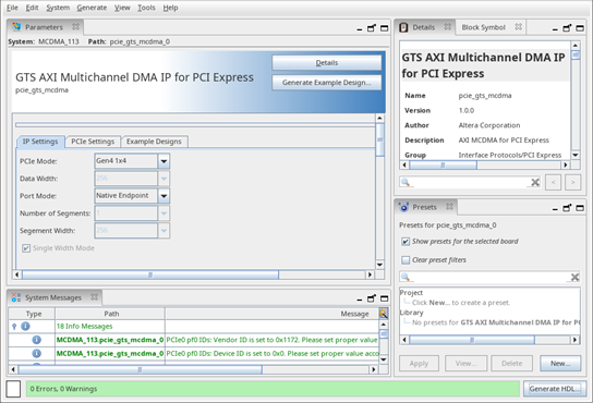
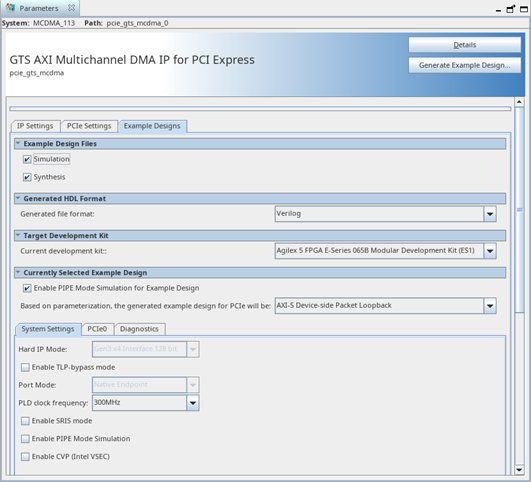
- Go to the Example Designs tab, and make the following selections:
- For Example Design Files, the Simulation and Synthesis options are turned on by default. Leave the settings in default, unless you do not need the simulation or synthesis files, and to reduce the design example generation time.
Note: The design example does not support simulation in this release. Turn off the Simulation option to reduce the design example generation time.
- For Generated HDL Format, only Verilog is supported in the current release.
- For Target Development Kit, select either the Agilex 5 FPGA E-Series 065B Modular Development Kit (ES1) or NONE to target the device selected for your current Quartus® Prime software project.
Note: If you select the development kit, the settings including the target device, pin assignments are included in the .qsf file of the generated design example, and you are not required to add them manually. These settings are board-specific for the development kit.Note: Agilex 5 FPGA E-Series 065B Modular Development Kit option is not supported for the Gen4 1x4 and Gen4 1x8 mode design examples in the current release.
- For Currently Selected Example Design, select a design example from a pulldown menu. Available design examples depend on the User Mode and User Interface settings in MCDMA Settings under the IP Settings tab.
 Available example design options for the MCDMA, BAM+MCDMA or BAM+BAS+MCDMA modes and AXI-S Interface type:
- AXI-S Packet Generate/Check
- AXI-S Device-side Packet Loopback
Available example design option for Bursting Master mode:- AXI-MM BAM EP Memory
Available example design option for BAM+BAS mode:- AXI-MM Traffic Generator/Checker
Table 30. Design Example Parameters Parameter Value Default Value Description Simulation On / Off On Design example simulation is not supported in the current release. Synthesis On / Off On When the Synthesis box is checked, all necessary file sets for synthesis are generated. When unchecked, only the Platform Designer system is generated. Generated file format Verilog Verilog HDL format. Current development kit - Agilex 5 FPGA E-Series 065B Modular Development Kit (ES1)
- None
Agilex 5 FPGA E-Series 065B Modular Development Kit (ES1) Selects a target FPGA development kit board.
Note: If an FPGA development board is selected, the target device used for generation is the one that matches the device on the development kit board.Note: Agilex 5 FPGA E-Series 065B Modular Development Kit option is not supported for the Gen4 1x4 and Gen4 1x8 mode design examples in the current release.Enable PIPE Mode Simulation for Example Design On / Off On When selected, PIPE mode simulation is enabled. Currently selected example design - AXI-S Device-side Packet Loopback
- AXI-S Packet Generate/Check
- AXI-MM Traffic Generator/Checker
- AXI-MM BAM EP Memory
AXI-S Device-side Packet Loopback Selects example design variant. Available design example variants are based on the User Mode and User Interface settings.
The list of design example options are:
MCDMA , BAM + MCDMA, or BAM + BAS + MCDMA modes and AXI-S interface type:- AXI-S Packet Generate/Check
- AXI-S Device-side Packet Loopback
MCDMA, BAM + MCDMA, or BAM + BAS + MCDMA modes and AXI-MM interface types:- AXI-MM DMA
Bursting Master mode:- AXI-MM BAM EP Memory
BAM + BAS mode:- AXI-MM Traffic Generator/Checker
Note:- Design example for Root Port mode is not supported.
Note: Design example generation includes the GTS AXI Streaming IP for PCI Express (intel_pcie_gts). Hence, the Example Designs tab includes the GTS AXI Streaming IP Parameter Editor. Some of the PCIe Interface parameters are automatically configured per the GTS AXI MCDMA IP parameter values and greyed out.Table 31. PCIe Interface Settings Parameters Parameter Value Default Value Description Hard IP Mode Gen4 x8 Interface 512-bit
Gen4 x4 Interface 256-bit
Gen3 x4 Interface 128-bit
Gen3 x4 Interface 128-bit Selects the PCIe Hard IP mode. Note: The mode value is passed from the GTS AXI MCDMA IP settings.Enable TLP-Bypass Mode On / Off Off Enables the TLP Bypass feature for the GTS AXI Streaming IP. Note: The TLP Bypass design example is not supported.Port Mode Root Port Native Endpoint
Native Endpoint Selects a PCIe mode for the GTS AXI Streaming IP. Note: The mode value is passed from the AXI MCDMA IP Settings.Note: The Root Port design example is not supported.PLD Clock Frequency Gen4 1x8: 500/450/400/350/300/250/200 MHz
Gen4 1x4: 350/300/250/200MHz
Gen3 1x4: 300/250/200MHz
300 MHz Selects the PLD clock frequency.
Enable SRIS Mode Off Off Enables the Separate Reference Clock with Independent Spread Spectrum Clocking (SRIS) feature. Enable PIPE Mode Simulation On / Off Off When on, this parameter enables the PIPE mode simulation. Enable CVP (Intel VSEC) On / Off Off Enables the CVP feature for the GTS AXI Streaming IP. - For Example Design Files, the Simulation and Synthesis options are turned on by default. Leave the settings in default, unless you do not need the simulation or synthesis files, and to reduce the design example generation time.
- Click on Generate Example Design to generate the design example variant. When the prompt asks you to specify the directory for your design example, you can accept the default directory, /pcie_gts_mcdma_0_example_design, or choose another directory. Then, click OK to kick off the design example generation.