GTS AXI Multichannel DMA IP for PCI Express* User Guide
5.1.3. AXI-MM Traffic Generator/Checker Design Example
This design example instantiates the Traffic Generator and Checker for the MCDMA module (BAS_TGC) that creates read and write transactions to exercise the Bursting Slave (BAS) module of the GTS AXI MCDMA IP configured in BAM+BAS mode. You can program the BAS_TGC by writing to its control registers through its Control and Status AXI-lite Subordinate interface. The traffic that it generates, and the traffic that the checker expects, is in a sequence of incrementing dwords.
For traffic generation, the host software allocates a block of memory in the PCIe space and then programs one of the windows in the Address Mapper to point to the allocated memory block. It also needs to set the start address, which is the base address of the selected space for write transactions, set the write count to the size of the block of the allocated memory block, and set the transfer size, before kick-starting the traffic generation. The number of completed transfers can be checked by reading the write count register.
For traffic checking, the host software sets the read address to point to the start address of the write transactions, set the read count to the size of the block of the allocated memory block, and set the transfer size, before kick-starting the traffic checker. The number of completed data checks and the number of errors occurred can be checked by reading the read count and read error count registers, respectively.
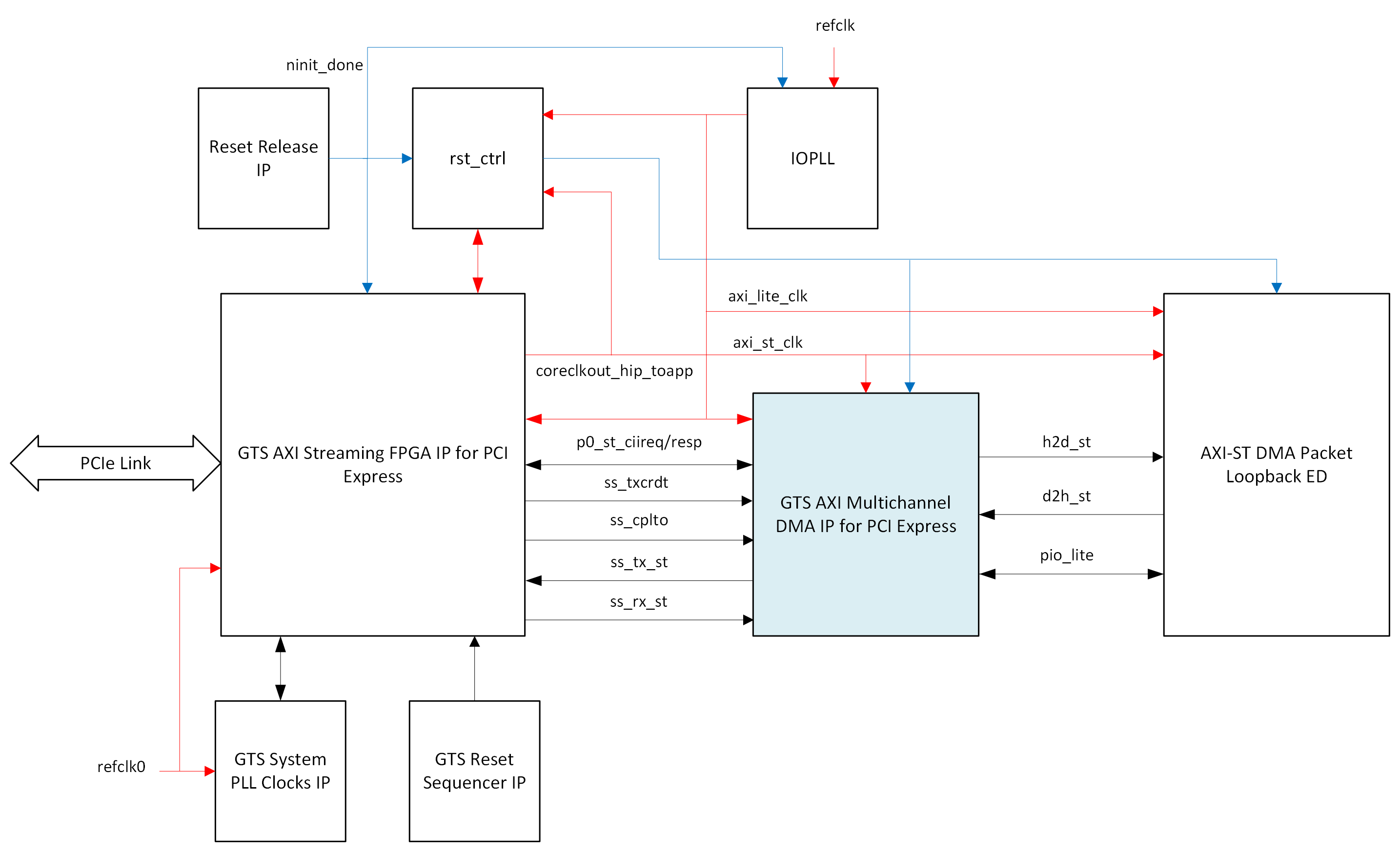
The AXI-MM Traffic Generator/Checker design example includes the following components:
| Design Components | Description |
|---|---|
| GTS AXI Multichannel DMA IP for PCI Express | Incorporates PCI Express (PCIe) into your design utilizing Altera's advanced PCIe hardened protocol stack, which encompasses the transaction, data link, and physical layers. It also includes optional components like Single Root I/O Virtualization (SR-IOV) for virtualization applications that demand high-bandwidth data transfer to and from host memory. This component converts the PCIe serial link transfer to the AXI Stream interface and directs the TLP data received to the GTS AXI Multichannel DMA IP. |
| GTS AXI Streaming IP for PCI Express | Facilitates efficient data transfer between the local FPGA and the host through multiple DMA channels over the PCIe link. Each DMA channel comprises a host-to-device (H2D) and a device-to-host (D2H) queue pair, operating on descriptor-based queues established by the driver software for data transfer. It is engineered to support standalone Endpoint or Root Port functionality, offering AXI-S and AXI-MM interfaces to the user logic. |
| GTS System PLL Clocks IP | This IP is required for a PCIe interface implementation on Agilex™ 5 devices to configure the reference clock for the System PLL and provides the clock signal for the p<n>_i_syspll_c0_clk of the GTS AXI Streaming IP.
Note: For more information, refer to the Implementing the GTS System PLL Clocks IP section in the GTS Transceiver PHY User Guide.
|
| GTS Reset Sequencer IP | This IP must be instantiated for each Agilex™ 5 FPGA side that uses transceivers for simulation and proper device operation. It provides the PMA Control Unit clock to the i_flux_clk clock of the GTS AXI Streaming IP.
Note: For more information, refer to the Implementing the GTS Reset Sequencer IP section in the GTS Transceiver PHY User Guide.
|
| Reset Release IP | This IP holds a control circuit in reset until the device has fully entered user mode. The FPGA asserts the INIT_DONE output to signal that the device is in user mode. It is required when using the GTS AXI Streaming IP.
Note: For more information on the Reset Release IP, refer to the Device Configuration User Guide: Agilex™ 5 FPGAs and SoCs.
|
| AXI-MM BAS Traffic Generator/Checker for MCDMA | This design example module implements a traffic generator and checker for the Bursting Slave (BAS) interface. Settings of the data transfer such as transfer size is configured via its AXI-lite Subordinate CSR interface, which is driven by the BAM interface in this design example. |
| BAM Interface BAR/PF/VF Interpreter for MCDMA | This module interprets the BAM address mapping to decode the physical function number, virtual function number and address of the incoming packet. The BAM packets are directed to the BAM memory and Traffic Generator/Checker module CSR interface. |
| BAM MEM | On-Chip Memory IP for bursting read/write operations that target the BAM interface. |
| rst_ctrl_0 | This module handles the reset and handshake signals of the GTS AXI Streaming IP for graceful entry and exit for each of the resets (cold, warm, etc.), especially when initiated by the host system. |
| IOPLL IP | This IP is required to configure the settings of the Agilex™ 5 I/O PLL to provide a 100MHz clock signal for the AXI-Lite interface in the design. |