AN 999: Drive-on-Chip with Functional Safety Design Example: Agilex™ 7 Devices
ID
823627
Date
7/04/2024
Public
1. About the Drive-on-Chip with Functional Safety Design Example for Agilex™ 7 Devices
2. Getting Started
3. Rebuilding the Drive-on-Chip Design
4. Functional Description of the Drive-On-Chip with Functional Safety Design Example for Agilex 7 Devices
5. HPS Channel Safety Software
6. Drive-on-Chip Design Recommendations and Disclaimers
7. Document Revision History for AN 999: Drive-on-Chip with Functional Safety Design Example for Agilex 7 Devices
2.1. Software Requirements for the Drive-On-Chip with Functional Safety Design Example for Agilex 7 Devices
2.2. Hardware Requirements for the Safe Drive-On-Chip with Functional Safety Design Example for Agilex 7 Devices
2.3. Downloading and Installing the Design
2.4. Installing Python
2.5. Creating an SD Card Image
2.6. Setting Up your Development Board for the Drive-On-Chip with Functional Safety Design Example for Agilex 7 Devices
2.7. Debugging and Monitoring the Drive-On-Chip with Functional Safety Design Example for Agilex 7 Devices with Python GUI
2.8. Looking into the Drive-On-Chip Output
3.1. Generating the Platform Designer System
3.2. Generating and Building the NiosV/g BSP for the Drive-On-Chip Design Example
3.3. Compiling the Hardware in the Intel Quartus Prime Software
3.4. Modifying the Motor Control Software Application
3.5. Generating .jic and .rbf files After Hardware Modifications
3.6. Recreate an SD Card Image
3.7. Modifying the HPS Safety Function Application
4.1. Drive-on-Chip Related Subsystems
The Drive-On-Chip for Functional Safety Design Example for Agilex 7 Devices blocks dniosv_subsystem, motor_model_subsystem_8, drive_subsystem_, and control_subsystem are the same as the Drive-On-Chip Example Design for Agilex 7 Devices but with some modifications and connections.
Figure 13. c-powerdown signal from the external safety logic logicThe connection between the motor_model subsystem and the esl_subsystem allows you to disconnect the motor from power supply if the system goes into safe state whenever the design detects an unsafe condition. The external safety logic asserts the signal to disconnect the motor.
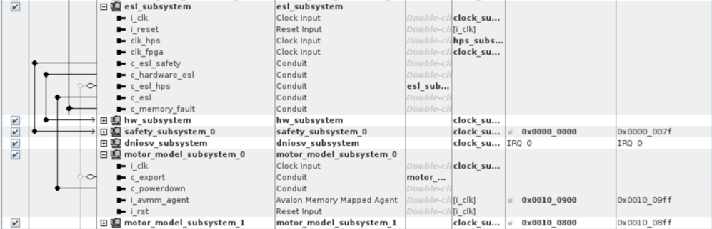
Figure 14. Bus connection from HPS to Drive-on-chip blocks using H2F-LW bridgeThe connection from the HPS2FPGA LW bridge (0xF900_0000) to all drive-on-chip subsystem blocks. This connection allows the HPS to change parameters of the motor control (refer to drive_on_chip.c functions). The connection allows the HPS to run speed estimation using the drive0 encoder (refer to qep_encoder.c)
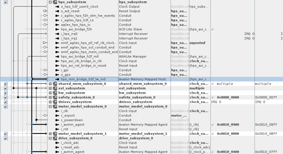
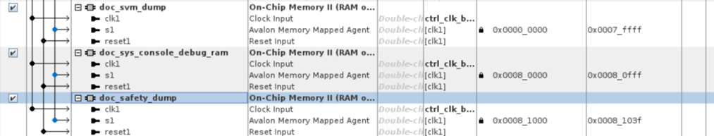
Figure 15. Additional dump memory in the Drive-on-Chip Control SubsystemAdditional doc_safety_dump memory in the control_subsystem to show safety-related values to the GUI. The HPS accesses the memory using functions from drive_on_chip.c in the HPS safety channel application. Then the GUI reads the values from memory via JTAG and shows them in the Safety tab.