2.2. Functional Description
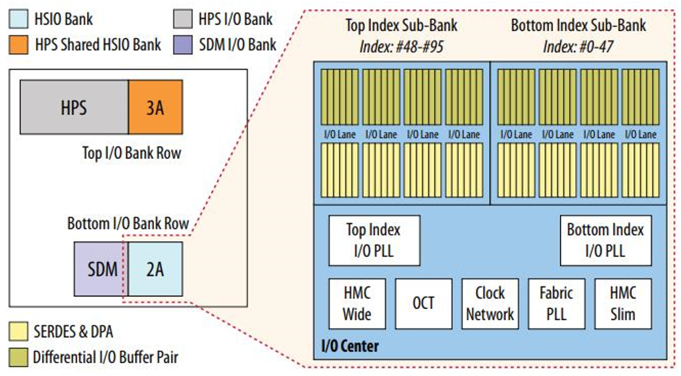
The PHY Lite for Parallel Interfaces FPGA IP for Agilex™ 3 C-Series devices utilizes the IO96 I/O banks in Agilex™ 3 C-Series devices. In general, each IO96 I/O bank has eight I/O lanes with 12 pins in each lane, providing a total of 96 pins per bank. Each bank contains pins that you can use for data and pins that are reserved for single-ended or differential strobe, reference clock, and RZQ. Some Agilex™ 3 C-Series packages may have partially bonded out I/O banks. The PHY Lite IP can still be used in these partially bonded out I/O banks, but with fewer than 96 pins available. For details about supported I/O banks, refer to the Agilex™ 3 C-Series Device Handbook. The following figure shows the Agilex™ 3 C-Series HSIO Bank Structure (Die Top View).
The following table shows package options for Agilex™ 3 C-Series devices.
| Device | Package (Key: HVIO / HSIO / HPSIO / Transceivers | ||||
|---|---|---|---|---|---|
| Ball Pitch: 0.5mm Grid Array Pattern: Standard MBGA: Micro Fineline BGA |
Ball Pitch: Variable Grid Array Pattern: Variable Pitch BGA VPBGA: Variable Pitch BGA |
||||
| M12A 484-pin MBGA 12mm x 12mm |
M16A 896-pin VPBGA 16mm x 16mm |
B18A 474-pin VPBGA 18mm x 18mm |
B18B 533-pin VPBGA 18mm x 18mm |
B23A 875-pin VPBGA 23mm x 23mm |
|
| A3C 025 | 160/72/0/0 | 160/48/0/0 | 160/96/0/0 | ||
| A3C 050 | 160/72/0/0 | 160/48/0/0 | 160/96/0/0 | ||
| A3C 065 | 160/72/0/0 | 160/48/0/0 | 160/96/0/0 | ||
| A3C 100 | 40/192/48/4 | 160/48/0/0 | 200/144/48/4 | ||
| A3C 135 | 40/192/48/4 | 160/48/0/0 | 200/144/48/4 | ||
For all devices in Package B18A, only the bottom sub-bank of the IO96 bank is bonded out. The following restrictions apply:
- The maximum number of data groups is 4.
- Place the RZQ pin in pin index 62 (lane 5).
- Place all data and strobe pins in lanes 4 – 7.