2.5. Advanced Link Analyzer Channel Designer
The Advanced Link Analyzer Channel Designer contains the following channel components:
- Stripline
- Coupled stripline
- Microstrip
- Coupled microstrip
- Coax
- RLGC transmission line
- Ideal transmission line
- Via model based on composite transmission line blocks
- Shunt and series capacitance
- Series inductance
- S-parameter model
- Near-end crosstalk extractions from a multiple-lane S-parameter
- Far-end crosstalk extractions from a multiple-lane S-parameter
- PCB stackup
A channel design can include one or multiple channel components. Advanced Link Analyzer Channel Designer can combine and generate Touchstone S-parameter models that can be used in link simulations. Advanced Link Analyzer Channel Designer provides user-friendly and integrated interfaces. The channel components and resulting channel models can be observed and analyzed using embedded plot functions or the Advanced Link Analyzer Channel Viewer.
In Advanced Link Analyzer, a 2-port single-ended channel model is generated internally for the following components:
- Stripline
- Microstrip
- Coax
- RLGC transmission line
- Ideal transmission line
- Via model based on composite transmission line blocks
- Shunt and series capacitance
- Series inductance
After the single-ended model is generated, Advanced Link Analyzer Channel Designer converts it into a 4-port differential-pair format by assuming that these two single-ended channels are uncoupled.
A full 4-port single-ended channel model is generated for the following components:
- Coupled stripline
- Coupled microstrip
- S-parameter model
Advanced Link Analyzer supports PCB stackup dataset entries in the design space. You can specify multiple PCB stackup datasets within a channel designer project. Stripline, microstrip, coupled stripline, and coupled microstrip models can be generated from substrate parameters within each individual channel designer or using one of the PCB stack datasets in the design space.
- n-port Single-ended S-parameter (Touchstone 1 and 2)
- n-port Mixed-mode S-parameter (Touchstone 2 only)
Channel cascading of all channel components, which include coupled stripline, coupled microstrip, and S-parameter channel components, are done in the 4-port level.
Starting the Advanced Link Analyzer Channel Designer
You can start Advanced Link Analyzer Channel Designer in two ways:
- Double-click adv_link_analyzer_channel_designer.exe
- Click Channel Designer in the Advanced Link Analyzer Control Module
The Advanced Link Analyzer Channel Designer’s graphical user interface is shown in the following figure.
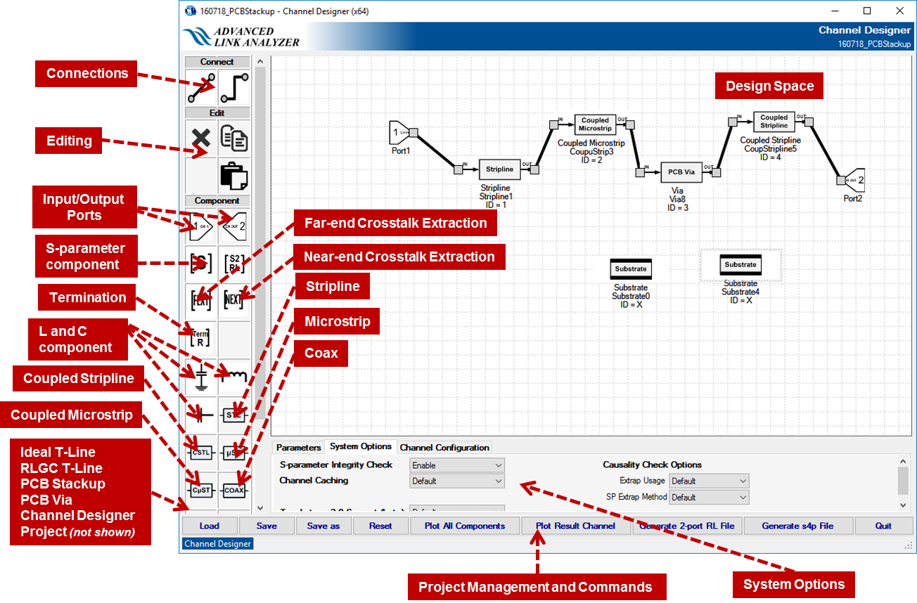
- Connect—Use the straight line or right-angled line to connect channel components
- Edit—Delete, copy, or paste channel components
- Component—Individual channel components to be added to the channel. See sessions below for details
- Design Space
- Parameters—Set up system level parameters
- S-parameter Max Frequency—Set the maximum frequency of the resulting channel model
- S-parameter Frequency Step—Set the frequency step of the resulting channel model
- Reference Impedance—Set the reference impedance of the resulting channel model
- System Options
- S-parameter Integrity Check—Select if checking channel integrity, such as passivity and causality, on the input S-parameter model. If Advanced Link Analyzer Channel Designer has issues opening or accessing certain S-parameter files, disable the channel integrity check to see if the issue is resolved.
- Channel Caching—Advanced Link Analyzer stores the recent read S-parameter model in memory for quicker accesses. Select Enable to enable the caching capability. Select Disable to disable the caching capability. Channel caching is enabled by default.
- Touchstone 2.0 Support—Use this menu to enable or disable Touchstone 2.0 S-parameter support.
- Causality Check Options
- SP Extrap Method—Use this menu to select S-parameter extrapolation method during causality checking. The default method is insertion loss fitting extrapolation method. The Last Amplitude Value option uses linear extrapolation and caps the amplitude at the last amplitude value from the S-parameter file.
- Extrap Usage—The default is to cap the amplitude of the extrapolation at the last amplitude value in the S-parameter file. The Always Apply option uses the values from the extrapolation without any restrictions.
- Project management and Commands
- Load—Load previously saved Channel Designer project
- Save/Save as—Save current project
- Reset—Clear all channel components
- Plot All Components—Plot all individual channel components in the Design Space using Advanced Link Analyzer Channel Viewer
- Plot Result Channel—Generate the result channel and plot its characteristics using Advanced Link Analyzer Channel Viewer
- Generate 2-port RL File—Generate 2-port return loss S-parameter file. This function allows you to extract or generate 2-port return loss S-parameter from your design. This feature also allows you to manipulate your 2-port return loss model by cascading with a channel file, for example, an S-parameter that represents a test fixture or changing/setting the termination impedance of the resultant 2-port return loss S-parameter.
- Generate s4p File—Generate the result channel and save it in a 4-port Touchstone S-parameter file
- Quit—Exit Advanced Link Analyzer Channel Designer
Constructing a Channel in Channel Designer
Similar to the Link Designer operations in Advanced Link Analyzer’s Control Module, a channel consists of one or more channel components between the input port (Port 1) and the output port (Port 2). After the channel components are placed into the workspace, click Connect to connect the components. In Connect mode, one or two connectors are shown on each component. Connect the channel components by dragging the line from one connector to another. Two types of connections are provided in Channel Designer: Right Angled Line and Straight Line.
The following rules of channel construction apply to the Channel Designer:
- The Input port (Port 1) has one output port or connector
- The Output port (Port 2) has one input port or connector
- A channel component has one input and one output port
- A connection between two components can be established from an output port to an input port
- An Input port cannot be connected directly to an Output port
A channel establishment checking algorithm runs constantly in the background, checking whether a channel is established for channel generation. When a channel is established between an input port and an output port, the link lines become bold. The User Interface figure above shows an established channel link.
Channel Components
The Channel Designer contains the following components:
- Port 1—Port 1 is the input port of the channel under construction.
- Port 2—Port 2 is the output port of the channel under construction.
S-parameter channel component
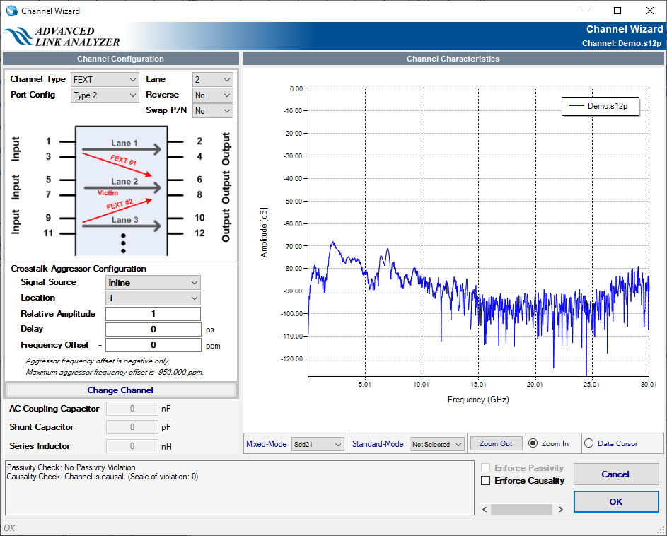
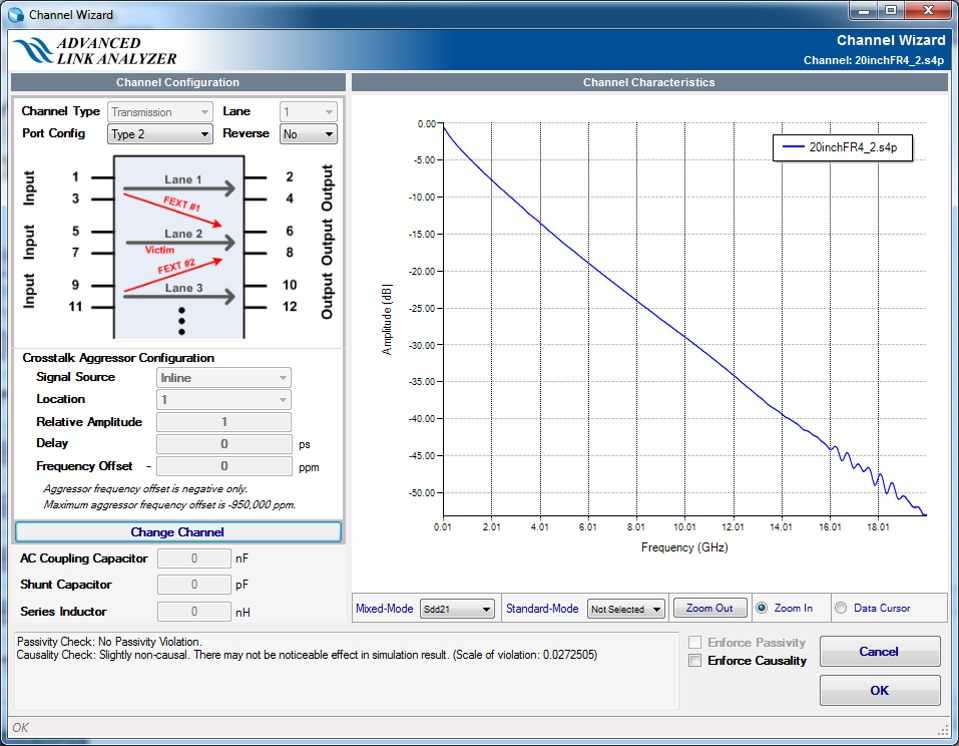
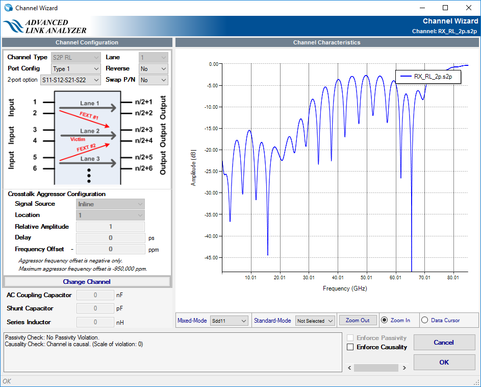
Use an S-parameter channel model file as part of the channel under construction. When you click the S-parameter icon, the Channel Wizard appears to help you configure the S-parameter file. Refer to the Advanced Link Analyzer Control Module’s Channel Wizard section for detailed usage. The following figure shows an example of the Channel Wizard:
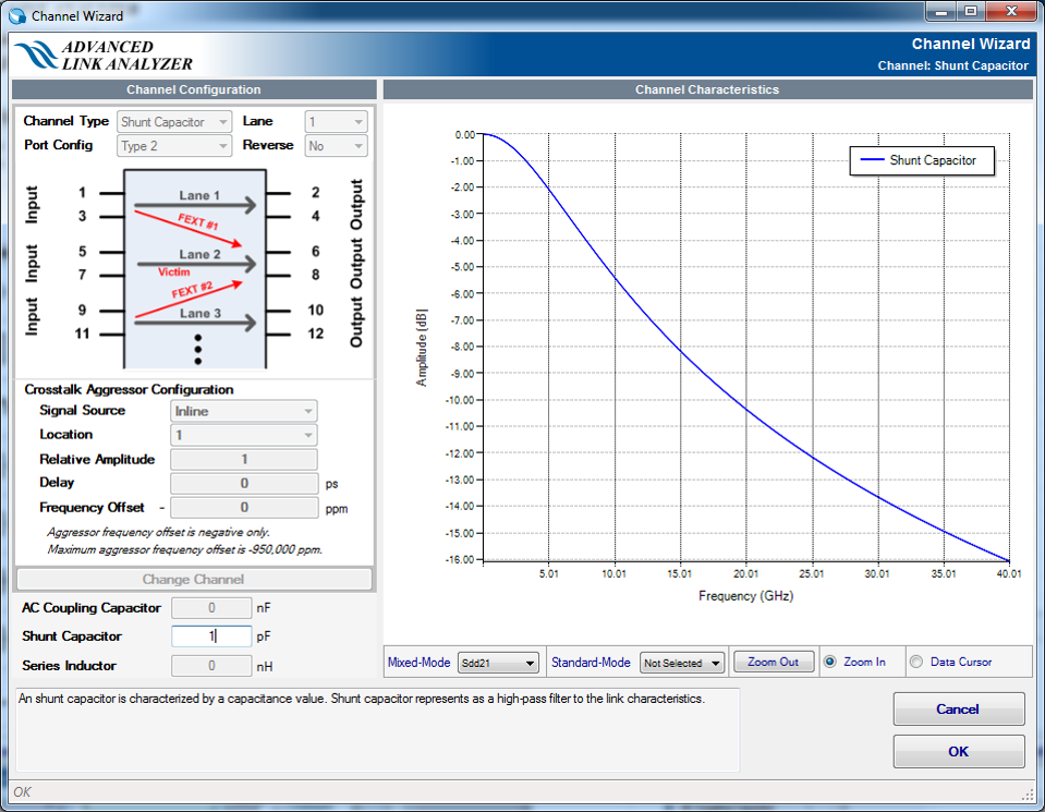
Capacitance and Inductance Model Components
You can insert the following capacitance and inductance components as part of the channel:
- Shunt capacitance
- Series capacitance—Listed in the Channel Wizard under the AC Coupling Capacitor
- Series Inductance
Advanced Link Analyzer Channel Designer uses the Channel Wizard to configure these capacitance and inductance components so you can input the capacitance and inductance values there. The following figure shows an example.
2-Port S-parameter Return Loss Channel Component
Stripline Component
A stripline uses a flat strip of metal that is sandwiched between two parallel ground planes. The insulating material of the substrate forms a dielectric. The width of the strip, the thickness of the substrate, and the relative permittivity of the substrate determine the characteristic impedance of the strip which is a transmission line. A typical stripline structure is shown in the following figure with these parameters:
- Input parameters
- W—Signal trace width (in various units)
- L—Signal trace length (in various units)
- Layer—PCB layer number where the signal trace is placed. This is only valid when PCB stackup dataset is used. The stripline cannot be placed on the top and bottom layers.
- T—Signal trace thickness (in various units)
- H—Separation between ground planes (in various units)
- Er (Dk)—Relative dielectric constant. Advanced Link Analyzer Channel Designer supports frequency dependent dielectric constant mapping.
- TanD (Df)—Dielectric loss tangent. Advanced Link Analyzer Channel Designer supports frequency dependent dissipation factor mapping.
- Cond—Conductor conductivity (S/m)
- Rough—Surface roughness (in various units)
- Mur—Relative permeability (no unit)
- Freq—Frequency where the Z0 (Impedance) and E-Eff (electrical length) are reported (in various units)
- Type—Substrate type. If "Current" is selected, the substrate characteristics are as specified in the GUI. If "SubstrateN" is selected, where N is associated with one of the PCB stackup datasets in the design space, the channel model is generated using the selected PCB stackup data.
- View PCB Stackup Table—Click this button to view the selected PCB stackup dataset. The PCB stackup is read-only.
- Output parameters
- Z0—Impedance at specified frequency Freq (Ohm)
- E-Eff—Electrical length (in various units)
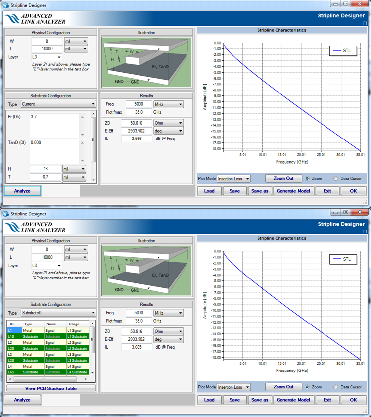
The channel component designer GUI can perform parameter unit conversion interactively. For example, you can change the length unit from mil to mm and the GUI automatically computes the length value with the new unit.
After entering the model parameters, click Analyze, and Channel Designer computes the frequency response of the current design. The integrated plotting engine can display the insertion loss or return loss characteristics. When you alter the model parameters, the GUI displays a message that indicates the channel characteristics may have changed. Click Analyze to redraw the channel characteristics. You can also load or save the component design for reuse in the future.
If you are satisfied with your design, click OK to save and close the component design GUI. If you click Exit or the window X button, you discard the design.
Microstrip Component
Microstrip is a type of electrical transmission line. It consists of a conducting strip separated from a ground plane by a dielectric layer known as the substrate. A typical microstrip structure is shown in the following figure with these parameters:
- Input parameters
- W—Signal trace width (in various units)
- L—Signal trace length (in various units)
- Layer—PCB layer number where the signal trace is placed. This is only valid when PCB stackup dataset is used. The microstrip can only be placed on the top and bottom layers.
- T—Signal trace thickness (in various units)
- H—Separation between ground planes (in various units)
- Er (Dk)—Relative dielectric constant. Advanced Link Analyzer Channel Designer supports frequency dependent dielectric constant mapping.
- TanD (Df)—Dielectric loss tangent. Advanced Link Analyzer Channel Designer supports frequency dependent dissipation factor mapping.
- Cond—Conductor conductivity (S/m)
- Rough—Surface roughness (in various units)
- Mur—Relative permeability (no unit)
- Freq—Frequency where the Z0 (Impedance) and E-Eff (electrical length) are reported (in various units)
- Type—Substrate type. If "Current" is selected, the substrate characteristics are as specified in the GUI. If "SubstrateN" is selected, where N is associated with one of the PCB stackup datasets in the design space, the channel model is generated using the selected PCB stackup data.
- View PCB Stackup Table—Click this button to view the selected PCB stackup dataset. The PCB stackup is read-only.
- Output parameters
- Z0—Impedance at specified frequency Freq (Ohm)
- E-Eff—Electrical length (in various units)
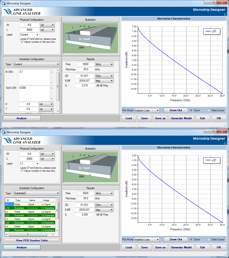
The channel component designer GUI can perform parameter unit conversion interactively. For example, you can change the length unit from mil to mm, and the GUI automatically computes the length value with the new unit.
After entering the model parameters, click Analyze, and Channel Designer computes the frequency response of the current design. The integrated plotting engine can display the insertion loss or return loss characteristics. When you alter the model parameters, the GUI displays a message that indicates the channel characteristics may have changed. Click Analyze to redraw the channel characteristics. You can also load or save the component design for reuse in the future.
If you are satisfied with your design, click OK to save and close the component design GUI. If you click Exit or the window X button, you discard the design.
Coax Component
A coax transmission line consists of two round conductors in which one completely surrounds the other. The two conductors are separated by a continuous solid dielectric. A typical coax structure is shown in the following figure with these parameters:
- Input parameters
- a—Diameter of inner conductor (in various units)
- b—Diameter of outer conductor (in various units)
- t—Thickness of outer conductor (in various units)
- Length—Length of the coax (in various units)
- Er (Dk)—Relative dielectric constant. Advanced Link Analyzer Channel Designer supports frequency dependent dielectric constant mapping.
- TanD (Df)—Dielectric loss tangent. Advanced Link Analyzer Channel Designer supports frequency dependent dissipation factor mapping.
- Cond (a)—Conductor conductivity of inner conductor (S/m)
- Cond (b)—Conductor conductivity of outer conductor (S/m)
- Freq—Frequency where the Z0 (Impedance) and E-Eff (electrical length) are reported (in various units)
- Output parameters
- Z0—Impedance at specified frequency Freq (Ohm)
- E-Eff—Electrical length (in various units)
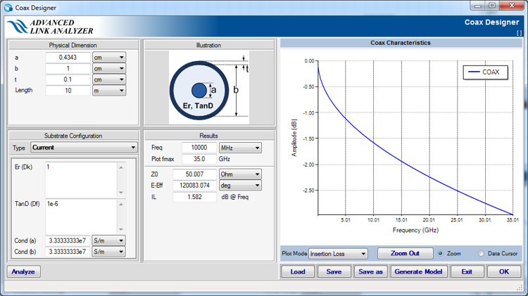
The channel component designer GUI can perform parameter unit conversion interactively. For example, you can change the length unit from mil to mm, and the GUI automatically computes the length value with the new unit.
After entering the model parameters, click Analyze, and Channel Designer computes the frequency response of the current design. The integrated plotting engine can display the insertion loss or return loss characteristics. When you alter the model parameters, the GUI displays a message that indicates the channel characteristics may have changed. Click Analyze to redraw the channel characteristics. You can also load or save the component design for reuse in the future.
If you are satisfied with your design, click OK to save and close the component design GUI. If you click Exit or the window X button, you discard the design.
RLGC Transmission Line Component
The channel is constructed with unit length RLGC models. A typical RLGC transmission line structure is shown in the following figure with these parameters:
- Input parameters
- L—Unit Length inductance (in various units)
- Rdc—Unit length DC resistance (in various units)
- Rac—Unit length skin-effect resistance (in various units)
- C—Unit length capacitance (in various units)
- Gdc—Unit length DC conductance (in various units)
- Gac—Unit length AC conductance (in various units)
- Length—Length of the coax (in various units)
- Freq—Frequency where the Z0 (Impedance) and E-Eff (electrical length) are reported (in various units)
- Output parameters
- Z0—Impedance at specified frequency Freq (Ohm)
- E-Eff—Electrical length (in various units)
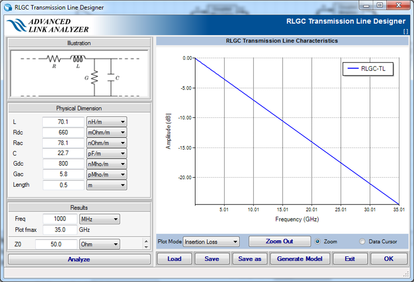
The channel component designer GUI can perform parameter unit conversion interactively. For example, you can change the length unit from mil to mm, and the GUI automatically computes the length value with the new unit.
After entering the model parameters, click Analyze, and Channel Designer computes the frequency response of the current design. The integrated plotting engine can display the insertion loss or return loss characteristics. When you alter the model parameters, the GUI displays a message that indicates the channel characteristics may have changed. Click Analyze to redraw the channel characteristics. You can also load or save the component design for reuse in the future.
If you are satisfied with your design, click OK to save and close the component design GUI. If you click Exit or the window X button, you discard the design.
Ideal Transmission Line Component
- Input parameters
- Z0—Target impedance (Ohm)
- Electrical length (in various units)
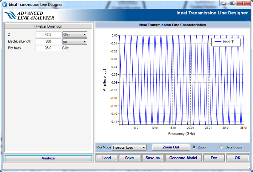
The channel component designer GUI can perform parameter unit conversion interactively. For example, you can change the length unit from mil to mm, and the GUI automatically computes the length value with the new unit.
After entering the model parameters, click Analyze, and Channel Designer computes the frequency response of the current design. The integrated plotting engine can display the insertion loss or return loss characteristics. When you alter the model parameters, the GUI displays a message that indicates the channel characteristics may have changed. Click Analyze to redraw the channel characteristics. You can also load or save the component design for reuse in the future.
If you are satisfied with your design, click OK to save and close the component design GUI. If you click Exit or the window X button, you discard the design.
Via Component
In printed circuit board design, a via consists of two pads in corresponding positions on different layers of the board. The pads are electrically connected by a hole through the board. In Advanced Link Analyzer Channel Designer, an analytical PCB Via model is constructed. A typical PCB via structure is shown in the following figure and the analytical via model structure is shown in the figure after that. The via is configured with the following parameters:
- Input parameters
- Via
- Impedance (Z3) (Ohm)
- Electrical Length (td3) (in various units)
- Pad 1
- Capacitance (C1) (in various units)
- Pad 2
- Capacitance (C2) (in various units)
- Via Stub 1
- Impedance (Z1) (Ohm)
- Electrical Length (td1) (in various units)
- Termination (R1) (in various units)
- Via Stub 2
- Impedance (Z2) (Ohm)
- Electrical Length (td2) (in various units)
- Termination (R2) (in various units)
- Via
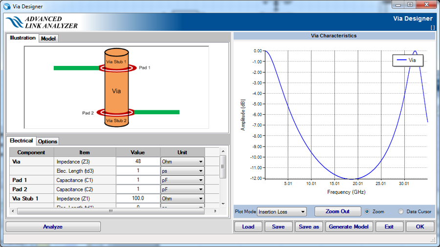
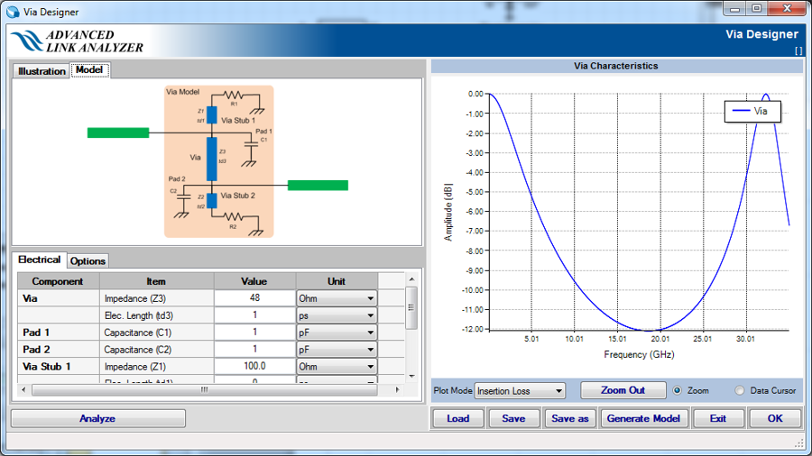
The channel component designer GUI can perform parameter unit conversion interactively. For example, you can change the length unit from mil to mm, and the GUI automatically computes the length value with the new unit.
After entering the model parameters, click Analyze, and Channel Designer computes the frequency response of the current design. The integrated plotting engine can display the insertion loss or return loss characteristics. When you alter the model parameters, the GUI displays a message that indicates the channel characteristics may have changed. Click Analyze to redraw the channel characteristics. You can also load or save the component design for reuse in the future.
If you are satisfied with your design, click OK to save and close the component design GUI. If you click Exit or the window X button, you discard the design.
CHDE Component
Advanced Link Analyzer Channel Design can use an existing Advanced Link Analyzer Channel Designer project as a channel component. When you click the CHDE icon, a file browser opens and lets you select an existing Channel Designer configuration file.
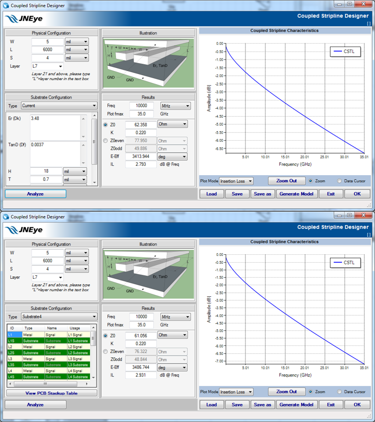
Coupled Stripline Component
A coupled stripline uses a pair of flat strip of metal that is sandwiched between two parallel ground planes. The insulating material of the substrate forms a dielectric. The width of the strip, the separation/space between the strips, the thickness of the substrate, and the relative permittivity of the substrate determine the characteristic impedance of the strip which is a transmission line. A typical coupled stripline structure is shown in the following figure with these parameters:
Input parameters:
- W—Signal trace width (in various units)
- L—Signal trace length (in various units)
- Layer—PCB layer number where the signal trace is placed. This is only valid when PCB stackup dataset is used. The coupled stripline cannot be placed on the top and bottom layers.
- S—Signal trace separation distance (in various units)
- T—Signal trace thickness (in various units)
- H—Separation between ground planes (in various units)
- Er (Dk)—Relative dielectric constant. Advanced Link Analyzer Channel Designer supports frequency dependent dielectric constant mapping.
- TanD (Df)—Dielectric loss tangent. Advanced Link Analyzer Channel Designer supports frequency dependent dissipation factor mapping.
- Cond—Conductor conductivity (S/m)
- Rough—Surface roughness (in various units)
- Mur—Relative permeability (no unit)
- Freq— Frequency where the Z0 (Impedance), K (coupling coefficient), Z0even (even mode impedance), Z0odd (odd mode impedance), and E-Eff (electrical length) are reported (in various units)
- Type—Substrate type. If "Current" is selected, the substrate characteristics are as specified in the GUI. If "SubstrateN" is selected, where N is associated with one of the PCB stackup datasets in the design space, the channel model is generated using the selected PCB stackup data.
- View PCB Stackup Table—Click this button to view the selected PCB stackup dataset. The PCB stackup is read-only.
Output parameters:
- Z0—Impedance at specified frequency Freq (Ohm)
- K— Coupling coefficient
- Z0even— Even mode impedance at specified frequency Freq (Ohm)
- Z0odd— Odd mode impedance at specified frequency Freq (Ohm)
- E-Eff—Electrical length (in various units)
The channel component designer GUI can perform parameter unit conversion interactively. For example, you can change the length unit from mil to mm, and the GUI automatically computes the length value with the new unit.
After entering the model parameters, click Analyze, and Channel Designer computes the frequency response of the current design. The integrated plotting engine can display the insertion loss or return loss characteristics. When you alter the model parameters, the GUI displays a message that indicates the channel characteristics may have changed. Click Analyze to redraw the channel characteristics. You can also load or save the component design for reuse in the future.
If you are satisfied with your design, click OK to save and close the component design GUI. If you click Exit or the window X button, you discard the design.
Coupled Microstrip Component
Coupled Microstrip is a type of electrical transmission line. It consists of a pair of conducting strips separated from a ground plane by a dielectric layer known as the substrate. A typical coupled microstrip structure is shown in the following figure with these parameters.
Input parameters:
- W—Signal trace width (in various units)
- L—Signal trace length (in various units)
- Layer—PCB layer number where the signal trace is placed. This is only valid when PCB stackup dataset is used. The coupled microstrip can only be placed on the top and bottom layers.
- S—Signal trace separation distance (in various units)
- T—Signal trace thickness (in various units)
- H—Separation between ground planes (in various units)
- Er (Dk)—Relative dielectric constant. Advanced Link Analyzer Channel Designer supports frequency dependent dielectric constant mapping.
- TanD (Df)—Dielectric loss tangent. Advanced Link Analyzer Channel Designer supports frequency dependent dissipation factor mapping.
- Cond—Conductor conductivity (S/m)
- Rough—Surface roughness (in various units)
- Mur—Relative permeability (no unit)
- Freq— Frequency where the Z0 (Impedance), K (coupling coefficient), Z0even (even mode impedance), Z0odd (odd mode impedance), and E-Eff (electrical length) are reported (in various units)
- Type—Substrate type. If "Current" is selected, the substrate characteristics are as specified in the GUI. If "SubstrateN" is selected, where N is associated with one of the PCB stackup datasets in the design space, the channel model is generated using the selected PCB stackup data.
- View PCB Stackup Table—Click this button to view the selected PCB stackup dataset. The PCB stackup is read-only.
Output parameters:
- Z0—Impedance at specified frequency Freq (Ohm)
- K— Coupling coefficient
- Z0even— Even mode impedance at specified frequency Freq (Ohm)
- Z0odd— Odd mode impedance at specified frequency Freq (Ohm)
- E-Eff—Electrical length (in various units)
The channel component designer GUI can perform parameter unit conversion interactively. For example, you can change the length unit from mil to mm, and the GUI automatically computes the length value with the new unit.
After entering the model parameters, click Analyze, and Channel Designer computes the frequency response of the current design. The integrated plotting engine can display the insertion loss or return loss characteristics. When you alter the model parameters, the GUI displays a message that indicates the channel characteristics may have changed. Click Analyze to redraw the channel characteristics. You can also load or save the component design for reuse in the future.
If you are satisfied with your design, click OK to save and close the component design GUI. If you click Exit or the window X button, you discard the design.
PCB Stackup Component
A printed circuit board (PCB) stackup describes the basic construction of a PCB. Specifically, the stackup defines the total number of PCB layers and the type and characteristics of each of these layers.
The PCB stackup structure is shown in the following figure.
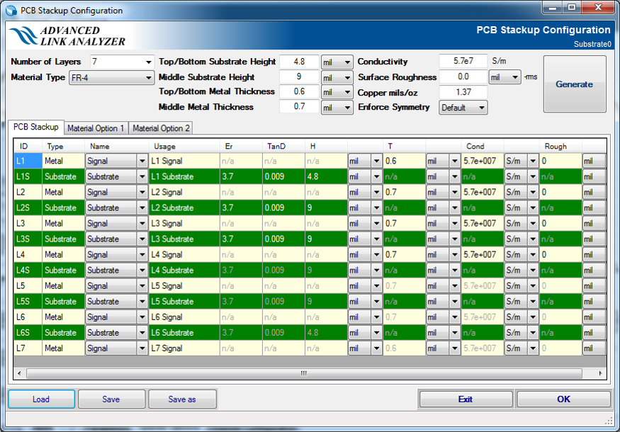
Input parameters:
- Number of Layers—Specify the number of PCB layers.
- Material Type—Select the type of PCB material. This sets the default relative dielectric constant (Er or Dk) and dielectric loss tangent (TanD or Df) associated with the selected PCB material. Each layer can have its own Er and TanD values. You can manually update the Er and TanD of each layer. The supported material types are:
- FR4—Default: Dk/Er = 3.8 and TanD/Df = 0.011
- Rogers—Default: Dk/Er = 3.4 and TanD/Df = 0.0027
- Nelco—Default: Dk/Er = 3.7 and TanD/Df = 0.009
- Megtron4—Default: Dk/Er = 3.8 and TanD/Df = 0.005
- Megtron6—Default: Dk/Er = 3.63 and TanD/Df = 0.004
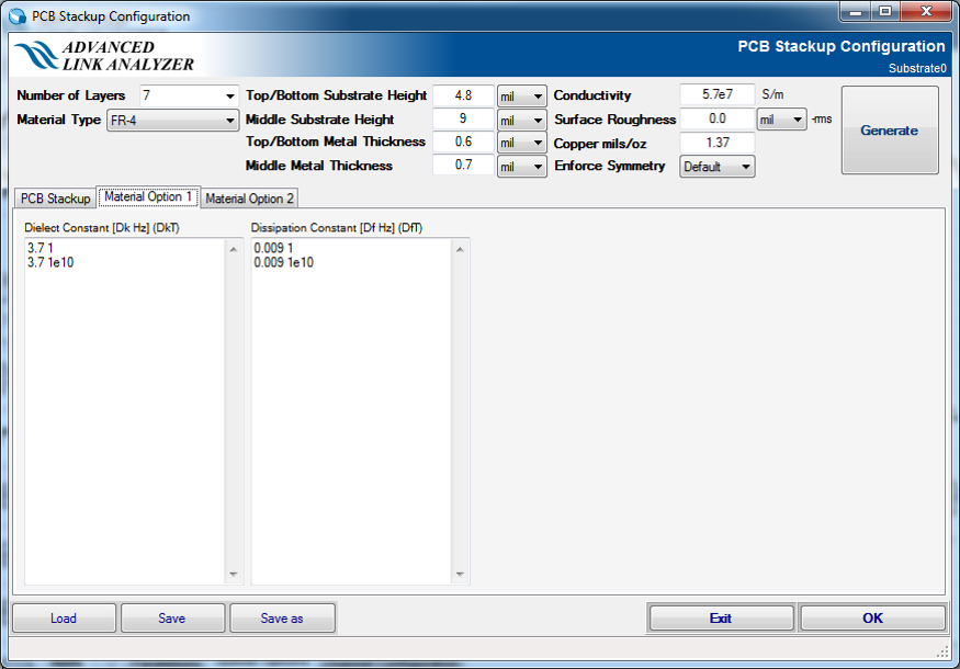
- Material Option 1—When selected, the Dk/Er and TanD/Df values are specified in the Material Option 1 tab page. This material option supports frequency-dependent Er/Dk and TanD/Df. See Figure 184 for an example.
- Material Option 2—When selected, the Dk/Er and TanD/Df values are specified in the Material Option 2 tab page. With this option, you can specify the Dk/Er and TanD/Df values for top/bottom and middle layers separately. This material option also supports frequency-dependent Er/Dk and TanD/Df. See Figure 185 for an example.
- Top/Bottom Substrate Height—This is the default substrate layer height value for the top and bottom layers when the PCB stackup table is initiated. You can select the appropriate length unit that suits their use.
- Middle Substrate Height—This is the default substrate layer height value for the middle PCB layers when the PCB stackup table is initiated. You can select the appropriate length unit that suits their use.
- Top/Bottom Metal Thickness—This is the default metal layer thickness for the top and bottom PCB layers. You can select the appropriate length unit that suits their use.
- Middle Metal Thickness—This is the default metal layer thickness for the middle PCB layers. You can select the appropriate length unit that suits their use.
- Conductivity—The default conductor conductivity (S/m) when the PCB stackup is initiated.
- Surface Roughness—The default surface roughness (in various units) when the PCB stackup is initiated.
- Copper mils/oz—The conversion factor when the metal thickness is specified in copper weight (oz)
- Enforce Symmetry—Choose to enforce the symmetry of the to-be-generated PCB stackup. If enabled, only the top half of the PCB stackup can be edited or modified; the lower-half PCB layers are automatically matched to the top layers. The default setting is Enable.
- Generate—Click Generate to generate the PCB stackup using the default values mentioned above.
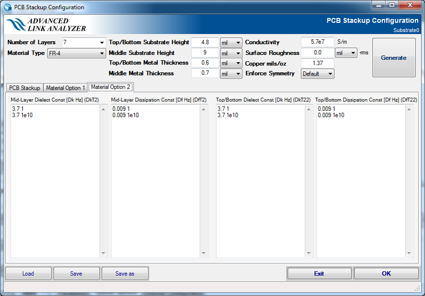
If you are satisfied with your design, click OK to save and close the component design GUI. If you click Exit or the window X button, you discard the design.
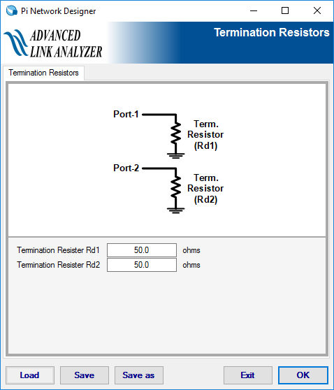
Termination Components
Use the termination component to set the termination impedance when generating or extracting 2-port return loss characteristics of your design. You must place it at the beginning or end of your link next to the Port 1 or Port 2, respectively.
Crosstalk Extraction Components
With multiple-lane S-parameters, in which the port number is greater than four, crosstalk characteristics can be embedded in the S-parameter data. While Advanced Link Analyzer can fully support and utilize the crosstalk data (both near-end and far-end crosstalk types), occasionally there is a need to extract the individual crosstalk characteristics for analysis or for other platforms' usage.
Advanced Link Analyzer Channel Designer uses the Channel Wizard GUI to guide the crosstalk data extraction with the following steps:
- Click NEXT for near-end crosstalk, or FEXT for far-end crosstalk.
- A file browser opens. Browse and open a multiple-lane S-parameter file.
- Advanced Link Analyzer Channel Wizard opens. Select crosstalk configurations such as port configuration, aggressor location, and victim lane.
- Click OK to place the crosstalk component into Channel Designer's design area.
The Channel Designer allows you to design your own crosstalk channel components by cascading the crosstalk component with other channel components. This feature can be useful in early design stages where the full link system is not fully developed for crosstalk extractions.