A newer version of this document is available. Customers should click here to go to the newest version.
2.1.4.3. Receiver Options
Receiver options provide further configuration and setting options for receivers.
- Termination tab—This section specifies receiver impedance.
Figure 51. Receiver Termination Configuration
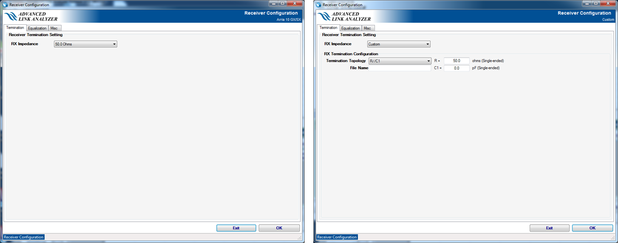
For selected Intel devices, use the RX Impedance pull-down menu to select a termination configuration. You can also customize the termination configuration by selecting the Custom option. When the Custom RX Impedance method is chosen, the termination can be configured as follows:
- Ideal RX termination—The receiver is ideal with a 50 ohms (single-ended) termination.
- Non-ideal RX termination—Select one of the following options:
- R—Receiver impedance is modeled as a resistance R ohms (single-ended).
- R//C1—Receiver impedance is modeled as an RC network with a parallel resistor (in ohms) and a capacitance (in pF).
- File Input (Frequency Real Imaginary)—Receiver impedance is modeled by a frequency-dependent complex impedance table described in the input file.
For an Intel receiver, the default termination configurations are automatically selected and specified.
- Equalization tab—For Intel® Arria® 10 GX/SX/GT, Stratix® V GX, and Arria® V GZ devices, the DFE model is embedded in the Advanced Link Analyzer with limited configurability. For Custom and PCI Express* 8GT/16GT receivers, the DFE configuration options are provided.
Equalization tab:
- DFE Tap Length—For supported Intel devices, you can manually reduce the DFE tap length. If the selected DFE tap length is larger than the device's original DFE tap length, the change is not applied in the simulation. For Intel® Arria® 10 devices, manually setting the DFE tap length disables floating DFE tap capability in the simulation.
Custom RX FFE/DFE tab:
- Algorithm—FFE/DFE is adapted using the LMS algorithm and its variations.
- DFE Tap Length—Number of DFE taps. This option is only available for Custom and PCI Express* 8GT receivers.
- FFE Tap Length—Number of FFE (feed-forward equalization) taps. This option is only available for Custom and PCI Express* 8GT/16GT receivers.
- Floating Tap—Enable or disable floating tap support. The default is Disable.
- Float Tap Length—Number of floating taps. If multiple-group floating taps is enabled, this specifies the number of floating taps in each group. If multiple-group is disabled, this specifies the total number of floating taps. The default is 4.
- Tap Location Type—Specifies how floating taps are organized. Group means that the floating taps are grouped together. In other words, you can have two groups of 3-tap DFE at separate locations. Individual means that floating taps can spread across the allowed range individually. The default is Group. Disable is not supported so do not select it.
- Number of Groups—Specifies the number of floating-tap groups. The default is 1.
- Max Float Tap Location—Specifies the allowable range of floating taps. The default is 64.
- Step Size—Step size of the LMS algorithm. This parameter controls the speed of the LMS adaptation. The default value is 0.01.
- Summation Node Model—Advanced Link Analyzer supports two generic/custom summation node modeling methods:
- 3dB Bandwidth (RC filter): Use a first-order RC filter to perform low-pass filtering of the DFE adjustment. Enter -1 to model the ideal summation node where the bandwidth is infinite.
- S-parameter: Use your S-parameter file to specify a pulse-shaping filter. Only the differential insertion loss (Sdd21) is applied in the pulse shaping.
- Reference Tap—Location of main cursor tap in the FFE.
- Override generic/standard device setting—For standard devices, for example, PCI Express* 8GT and 16GT, the DFE tap length, coefficient range, and summation node bandwidth are pre-configured within the device model. Turn on this option if you want to simulate these devices with custom settings.
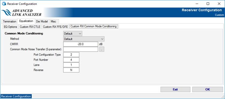
Custom RX Common Mode Conditioning tab:
- Common Mode Conditioning—Enable or Disable common mode noise conditioning. The default value is Disable.
- Method—Advanced Link Analyzer supports these methods. The default value is CMRR (Scalar) method.
- CMRR (Scalar): Filters the common mode noise by scaling its amplitude by the value specified in the CMRR text box.
- Common Mode Noise Transfer (S-parameter): Filters the common mode noise by an S-parameter specified in the Common Mode Noise Transfer (S-parameter) text box.
- CMRR—Common Mode Rejection Ration value in dB.
- Common Mode Noise Transfer (S-parameter)—Specifies transfer function applicable to the common mode noise. You can click the button next to the text box to select an S-parameter. Advanced Link Analyzer Channel Wizard helps you to configure the S-parameter values:
- Port configuration type
- Port number
- Lane selection
- Signal flow direction
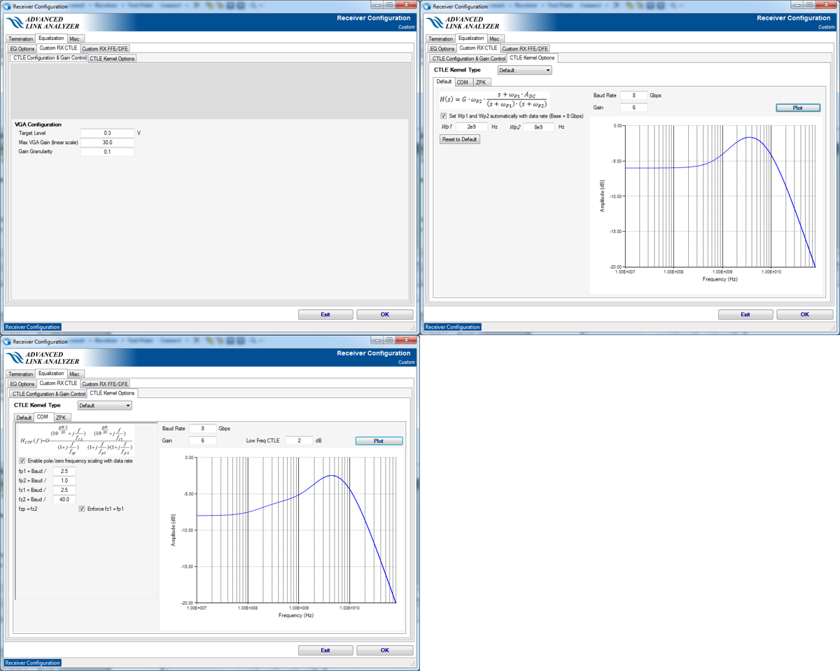
Custom RX CTLE tab:
- CTLE Configuration & Gain Control tab:
- VGA Configuration
- Target Level: The target voltage level of VGA output
- Max VGA Gain (linear scale): The maximum VGA gain in linear scale
- Gain Granularity: When VGA is in auto mode, the step size of VGA gain
Note: Custom RX's VGA has flat gain across frequencies. - VGA Configuration
- CTLE Kernel Options tab:
-
CTLE Kernel Type: Choices are Default and COM. Default method uses PCI Express* 8GT reference CTLE model which scales with data rate relative to 8 Gbps, i.e. PCI Express* 8GT's data rate. COM method uses IEEE 802.3cd COM reference CTLE model. Advanced Link Analyzer allow users to modify the frequency divider of pole and zero locations and frequency scaling.
-
- Misc tab—Reserved. This tab is blank.