Intel® Hyperflex™ Architecture High-Performance Design Handbook
A newer version of this document is available. Customers should click here to go to the newest version.
2.4.2.9.4. Memory Mixed Port Width Ratio Limits
When migrating a design that uses invalid port width ratios for Intel® Hyperflex™ architecture FPGAs, modify the RTL to create the desired ratio.
To create a functionally equivalent design, create and combine smaller memories with valid mixed port width ratios. For example, the following steps implement a mixed port width ratio:
- Create two memories with ¼ mixed port width ratio by instantiating the 2-Ports memory IP core from the IP Catalog.
- Define write enable logic to ping-pong writing between the two memories.
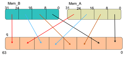
- Interleave the output of the memories to rebuild a 1/8 ratio output.
This example shows the interleaving of two memories and the write logic. The chosen write logic uses the least significant bit of the write address to decide which memory to write. Even addresses write in memory mem_A, odd addresses write in memory mem_B.
Because of the scheme that controls writing to the memories, carefully reconstruct the full 64-bit output during a write. You must account for the interleaving of the individual 8-bit words in the two memories.
This example shows the descrambled output when attempting to read at address 0h0.
The following RTL examples implement the extra stage to descramble the data from memory on the read side.
Top-Level Descramble RTL Code
module test
#(	parameter WR_DATA_WIDTH = 8,
		parameter RD_DATA_WIDTH = 64,
		parameter WR_DEPTH = 64,
		parameter RD_DEPTH = 4,
		parameter WR_ADDR_WIDTH = 6,
		parameter RD_ADDR_WIDTH = 4
)(
	data, wraddress, rdaddress,	wren,
	wrclock, rdclock,	q
);

input	[WR_DATA_WIDTH-1:0]	data;
input	[WR_ADDR_WIDTH-1:0]	wraddress;
input	[RD_ADDR_WIDTH-1:0]	rdaddress;
input		wren;
input		wrclock;
input		rdclock;
output	[RD_DATA_WIDTH-1:0]	q;

wire wrena, wrenb;
wire [(RD_DATA_WIDTH/2)-1:0] q_A, q_B;

memorySelect memWriteSelect (
	.wraddress_lsb(wraddress[0]),
	.wren(wren),
	.wrena(wrena),
	.wrenb(wrenb)
);

myMemory mem_A (
	.data(data),
	.wraddress(wraddress),
	.rdaddress(rdaddress),
	.wren(wrena),
	.wrclock(wrclock),
	.rdclock(rdclock),
	.q(q_A)
);

myMemory mem_B (
	.data(data),
	.wraddress(wraddress),
	.rdaddress(rdaddress),
	.wren(wrenb),
	.wrclock(wrclock),
	.rdclock(rdclock),
	.q(q_B)
);

descrambler #(
	.WR_WIDTH(WR_DATA_WIDTH),
	.RD_WIDTH(RD_DATA_WIDTH)
) outputDescrambler (
	.qA(q_A),
	.qB(q_B),
	.qDescrambled(q)
);

endmodule
Supporting RTL Code
module memorySelect (wraddress_lsb, wren, wrena, wrenb);
	input wraddress_lsb;
	input wren;
	output wrena, wrenb;

	assign wrena = !wraddress_lsb && wren;
	assign wrenb = wraddress_lsb && wren;
endmodule

module descrambler #(
	parameter WR_WIDTH = 8,
	parameter RD_WIDTH = 64
) (
	input [(RD_WIDTH/2)-1 : 0] qA,
	input [(RD_WIDTH/2)-1 : 0] qB,
	output [RD_WIDTH:0] qDescrambled
);

	genvar i;
	generate
  	for (i=WR_WIDTH*2; i<=RD_WIDTH; i += WR_WIDTH*2) begin: descramble
   	  assign qDescrambled[i-WR_WIDTH-1:i-(WR_WIDTH*2)] = qA[(i/2)-1:(i/2)-WR_WIDTH];
      assign qDescrambled[i-1:i-WR_WIDTH] = qB[(i/2)-1:(i/2)-WR_WIDTH];
    end
  endgenerate

endmodule