Video and Vision Processing Suite Intel® FPGA IP User Guide
A newer version of this document is available. Customers should click here to go to the newest version.
23.3.3. External Memory for Warp IP
Memory Space Allocation in External Memory
| Buffer Space Configuration | Region Size (MB) | Memory Region Required | Alignment (multiples of) |
|---|---|---|---|
| SD buffer size (1024x1024) | 24 | 0x0180_0000 | 0x0200_0000 |
| HD buffer size (2048x2048) | 96 | 0x0600_0000 | 0x0800_0000 |
| UHD buffer size (4096x4096) | 384 | 0x1800_0000 | 0x2000_0000 |
| Buffer Space Configuration | Region Size (MB) | Memory Region Required | Alignment (multiples of) |
|---|---|---|---|
| SD buffer size (1024x1024) | 16 | 0x0100_0000 | 0x0100_0000 |
| HD buffer size (2048x2048) | 64 | 0x0400_0000 | 0x0400_0000 |
| UHD buffer size (4096x4096) | 256 | 0x1000_0000 | 0x1000_0000 |
The IP passes the base address of the memory region allocated to the frame buffers to the software API using the ram_addr element in the structure.
The memory region that the coefficient tables require is related to the number of warp engines, the resolution of the images, and the type of warp. The IP only requires this memory region when you turn off Use easy warp.
| Warp Engines | Region Size (MB) | Memory Region Required | Alignment (multiples of) |
|---|---|---|---|
| 1 | 16 | 0x0100_0000 | 0x0100_0000 |
| 2 | 32 | 0x0200_0000 | 0x0200_0000 |
Bandwidth to External Memory
The performance of the interface from the Warp IP to the external memory is important for the correct operation of a system using the Warp IP.
The Warp IP generates a substantial amount of memory traffic. It has four video streams passing to and from external memory. In addition, each engine has three read streams to access the coefficient tables. All these streams combine to make Warp IP memory accesses complex. The streams affect how much efficiency you can obtain when accessing DDR4 memory.
The Warp IP memory controller mitigates potential inefficiencies caused by these complex access patterns. It uses burst lengths of 8 beats for all its read and write accesses to improve the burst performance to DDR4 memory. It also attempts to cluster individual read and write bursts together to eliminate some of the issues with read and write turnaround dead time at the DDR4 interface.
These memory access patterns depend on the image transform that you apply. Some complex image transforms may reduce memory traffic because of the skip region functionality. One of the worst transforms for generated memory traffic is a unity warp that gives a 1:1 mapping between input and output pixels.
The operation of the Warp IP is easier to predict when it is the only user of the DDR4 memory in a system. Ensure the Warp IP is the only high bandwidth user of the DDR4 memory in a system. When other high bandwidth accesses are made to the memory at the same time as the Warp IP, ensure that any interactions don’t adversely affect performance.
Memory Interface Bandwidth Requirements
Intel approximates the worst case burst data rate through the IP’s memory interface assuming four video streams plus each engine reading three channels of coefficient data. Each 30-bit pixel is stored in memory as a 32-bit word.
For a UHD system running at 60 fps the worst case burst data rate is approximately 72 Gbps.
| Resolution | Frame Rate (fps) | Maximum Burst Data Rate (Gbps) |
|---|---|---|
| 3840x2160 | 60 | 72 |
| 3840x2160 | 30 | 36 |
| 1920x1080 | 60 | 18 |
When you turn on Use easy warp, approximate the worst case burst data rate through the Warp IP’s memory interface assuming two video streams. For a full HD system running at 60 fps the worst case burst data rate is approximately 8.5 Gbps.
Intel references these burst data rates to the memory interface of the IP. The total data rates available are affected by other factors outside of the IP such as the performance of the interconnect fabric and the efficiency of the memory controller.
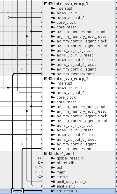
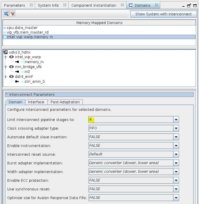
Example system sharing access to memory
In this example system the Warp IP shares the DDR4 interface with a frame buffer in a system that processes UHD frames at 60 fps. The system runs on an Intel Arria 10 GX Development Kit with the DDR4 EMIF running a 2,133 MHz interface to a DDR4 memory.
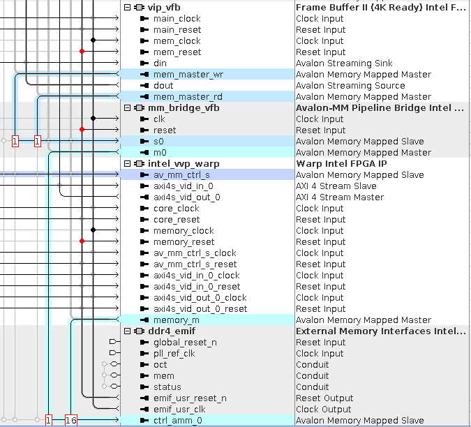
For this system to work:
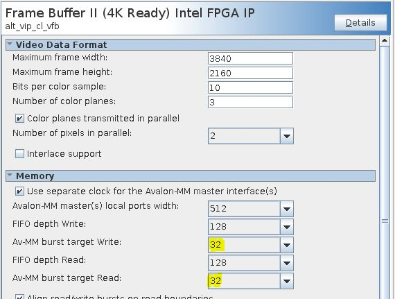
- Configure Frame Buffer to use bursts of 32 beats for read and write.
- Configure Frame Buffer to use read and write FIFO depths of 128
- Set the arbitration weighting at the front end of the DDR4 EMIF to 16:1 in favor of the Warp IP (versus the Frame Buffer’s read and write interfaces connected through the mm_bridge_vfb component).
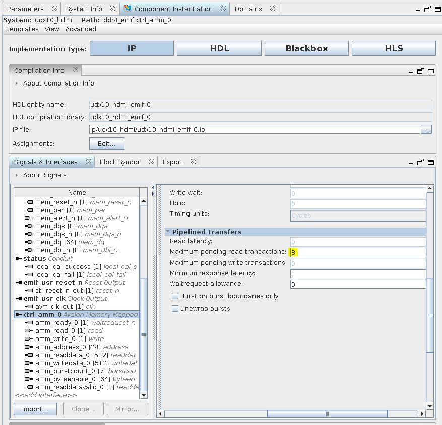
- Set the Maximum pending read transactions parameter in the pipelined transfers section of the Avalon Memory Mapped agent port to be at 8.
- Set Limit interconnect pipeline stages to for the domain at the front end of the DDR4 EMIF to 4.
Multiple Warp IPs sharing access to memory