AN 875: Intel® Stratix® 10 E-Tile PCB Design Guidelines
ID
683262
Date
3/12/2019
Public
2.3.2.2. Return Loss
You must optimize the PCB trace impedance to achieve a better return loss or less signal reflection. Factors that determine the PCB impedance Z0 value for a better RL performance are:
- Elements in the end-to-end channels:
- Device packages
- PCB vias
- Connectors
- Cables
- DC block caps (if they exist)
- PCB stackup and the dielectric and copper materials
Picking the PCB impedance Z0 that gives the minimum impedance fluctuation (discontinuity) with all other elements of the channel is the key for transferring the signal from one end of the channel to the other while minimizing the signal reflection.
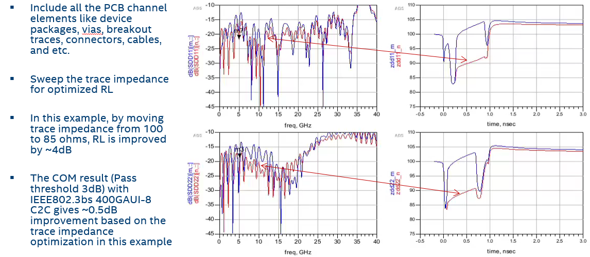
The following figure shows an example of PCB trace impedance optimization. From the blue to red performance curves (insertion loss, return loss and time domain reflectometry (TDR) at both ends), it appears that a reduction in the impedance fluctuation eventually leads to a return loss improvement.
Figure 7. Example of PCB Trace Impedance Optimization