AN 875: Intel® Stratix® 10 E-Tile PCB Design Guidelines
2.3.3.1. FPGA PCB Breakout Design and Reference
This section focuses on the FPGA PCB breakout routing for high-density serial channel designs beyond 10 Gbps.
Refer to the AN-651-1.0 application note for preliminary breakout routing study.
Link to AN-651-1.0: PCB Breakout Routing for High-Density Serial Channel Designs Beyond 10 Gbps
The Intel® Stratix® 10 E-Tile differential RX/TX balls are completely shielded with ground balls, as compared to previous RX/TX balls being diagonally placed without ground ball shielding. The FPGA BGA/pin pitch is 1mm. There are some changes to breakout routing techniques in AN-651 as described below to better impedance matching.
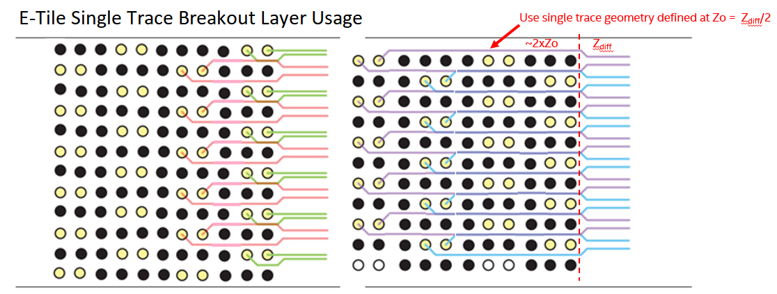
The single trace breakout study in AN-651 does not consider ~47 ohm Zo (but uses a 51.3 ohm Zo instead), so there is an impedance discontinuity at the boundary between the single trace breakout and the differential routing segments. With ~47-ohm for the single trace breakout, the differential impedance can be maintained at around ~94 ohm when crossing the boundary. The single trace breakout can still be an option with the differential impedance matching technique mentioned above when the ground reference coverage for differential breakout traces becomes an issue due to large optimized via anti-pads for a high-Dk and high-layer-count PCB.
Another benefit with the single trace breakout is that the breakout layer assignment is not constrained by the back-drill effectiveness mentioned in AN-651 due to adequate via-to-copper clearance for the back-drill.
- Single trace Zo = 51.3 ohm, Zdiff = ~102.6 ohm with loosely coupled P/N traces.
- Use widened single trace with Zo = Zdiff / 2 to match the differential impedance.
- Via impedance also plays a major role in the loss performance in the study.