2.3.3.3. Crosstalk - NEXT and FEXT in Differential Pairs
In PCB layout, the typical crosstalk sources are:
- PCB BGA via
- Distance between vias, nearby ground vias, and via barrel length parallelism
- PCB via for layer transition and DC blocking capacitors
- Distance between vias, nearby ground vias, and via barrel length parallelism
- PCB traces
- Edge coupled micro-strip lines
- Pair-to-pair airgap, trace to reference plane distance, and trace coupling length, based on simulation, all combine to obtain FEXT < -50 dB, NEXT < -60 dB
- Edge coupled strip lines
- Pair-to-pair airgap, trace to reference plane distance, and trace coupling length, based on simulation, all combine to obtain FEXT < -50 dB, NEXT < -60 dB
- Edge coupled micro-strip lines
- Connectors
- Vendors, types, pin assignments, footprints, etc.
The other source of crosstalk is the package as discussed in the section titled Package Loss. The achieved package crosstalk for the Intel® Stratix® 10 E-Tile is less than -60 dB for NEXT and less than -50 dB for FEXT.
Crosstalk at BGA VIA
There are multiple factors affecting the crosstalk at a BGA via, including:
- Pin assignment
- How close the signal pins are to one another
- How far the signal pins are from reference (ground) pins
- Routing layer assignment
- Using a routing layer closer to the BGA chip results in shorter via barrels and less coupling among the vertical signal vias.
- Via anti-pad size
- Tuning the via anti-pad with larger sizes to mitigate the low via impedance issue can also increase the crosstalk due to less coupling to the reference. Include the crosstalk effect during the via impedance optimization as a design trade-off.
- PCB Stackup
- More reference planes within the same stackup thickness (i.e. denser reference planes) provide a higher coupling to reference, resulting in less crosstalk.
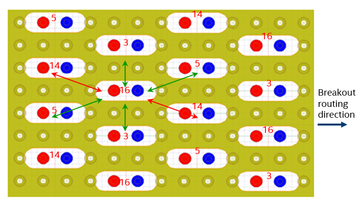
The following figure shows an example of a routing layer assignment for less BGA via crosstalk. A typical breakout layer assignment for high-speed differential signals is illustrated. There are six adjacent signal via pairs acting as crosstalk sources in this example. The worst coupling pair depends on the number of grounds between the columns/rows (vertical ground vias). Coupling between breakout vias in the bottom layers gives significant crosstalk due to long via barrel parallelism. The crosstalk due to this parallelism from the six neighbors has also been illustrated in the figure.
Figure 22. BGA Via Barrel Parallelism and Crosstalk in Routing Layers Assignment
Strategy to Reduce Crosstalk among BGA Vias
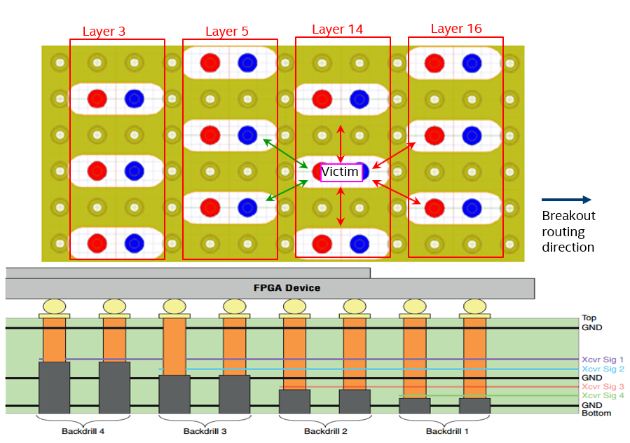
Here are some tips to reduce the crosstalk among BGA vias (illustrated in the figure below):
- Stagger breakout layers for adjacent signals and reduce the via parallelism.
- For an n-layer board:
- Use adjacent signal vias with breakout on layers i and j where i+j <= n+1.
- Single trace breakout may be needed for drill to trace tolerance/margin.
Figure 23. Strategy to Reduce BGA Vias Crosstalk in Routing Layer Assignment
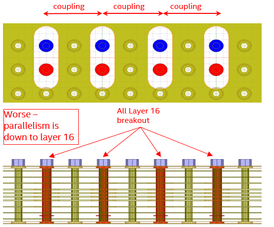
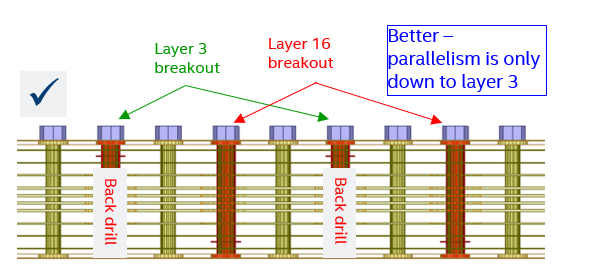
The figure below shows the final breakout layer assignment for the example shown in the figure titled BGA Via Barrel Parallelism and Crosstalk in Routing Layers Assignment above. In this assignment, the crosstalk to the six adjacent high-speed differential signal via pairs has been improved. In the example, an 18-layer board has been used and via barrel parallelism from the neighbors has been reduced. Single-ended trace breakout may be needed for drill-to-trace tolerance and also back-drill-to-trace tolerance.
Figure 24. Final Breakout Layer Assignment for BGA Via Crosstalk Reduction