5.5. Clock Connections in Synchronous Ethernet Operation
The Synchronous Ethernet standard, described in the ITU-T G.8261, G.8262, and G.8264 recommendations, requires that the TX clock be filtered to maintain synchronization with the RX reference clock through a sequence of nodes. The expected usage is that user logic drives the transceiver reference clocks with a filtered version of the RX recovered clock signal, to ensure the receive and transmit functions remain synchronized. In this usage model, a design component outside the IP core performs the filtering off chip.
In the diagram below, the recovered clock outputs from the IPs can be connected to the off-chip cleanup PLL using tile PIN. In F-tile, the recovered clock from the FGT PMA can be driven to dedicated clock output pins on the tile itself. Each F-tile has only two such clock outputs: FGT QUADs 2 and 3. Each has one dedicated clock output pin (Refclk8/9).
The primary and backup cleanup clocks come from recovered clock output pins from a pair of ports connected to remote stations on the same SyncE network, with the transceiver reference clock is sourced from the output of the cleanup PLL.
In the diagram below, out_cdr_clk0 is the clock that goes to off-chip cleanup PLL.
Implementation of Synchronous Ethernet (SyncE) Operation
The output frequency is equal to the nominal incoming refclk divided by the pre-divider on the RX path:o_cdr_divclk=refclk/N.
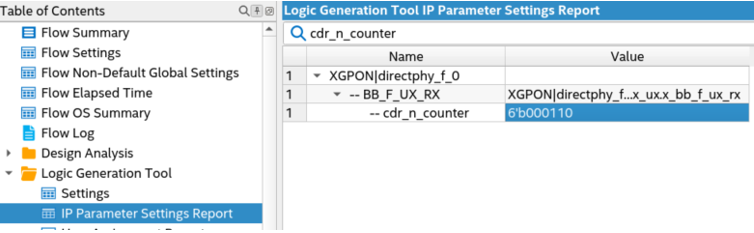
To retrieve the N divider value, follow the steps below:
- Compile the design.
- Open Compilation Report, then go to Logic Generation Tool > IP Parameter Settings Report.
- Search cdr_n_counter.
- [optional] You can also search cdr_f_ref_hz to double confirm the input reference clock frequency.
Figure 28. Retrieve the N divider Value
| NRZ/PAM4 | Input Refclk (MHz) | N divider | Output Recovered Clk (MHz) |
|---|---|---|---|
| NRZ | 156.25 | 4 | 39.0625 |
| 156.25 | 6 | 26.0417 | |
| 312.5 | 8 | 39.0625 | |
| 312.5 | 12 | 26.0417 | |
| 322.265625 | 12 | 26.8554688 | |
| PAM4 | 156.25 | 6 | 26.0417 |
| 312.5 | 12 |
Example Design Generation of Synchronous Ethernet Operation
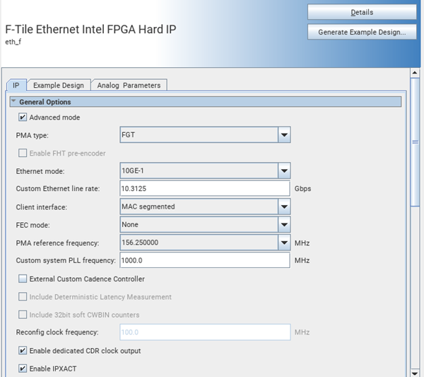
- To generate the example design, after selecting the Enable dedicated CDR Clock Output in the IP parameter editor, go to Example Design tab.
- In the Select Design parameter under Available example Designs, you can select the following options:
Figure 30. Select Designs Example Design
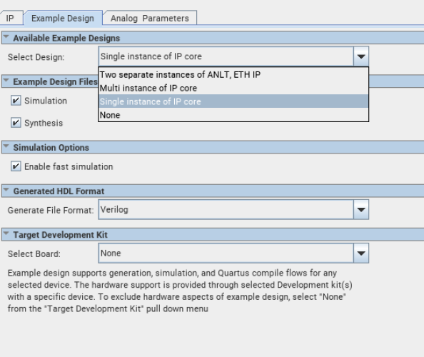
- Two separate instances of AN/LT, ETH IP
- Multi instance of IP core
- Single instance of IP core
- None
Note: The multi instance of IP core is not supported when Enable dedicated CDR Clock Output is set to on.