External Memory Interfaces (EMIF) IP User Guide: Agilex™ 3 FPGAs and SoCs
A newer version of this document is available. Customers should click here to go to the newest version.
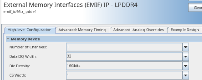
6.10.2.1. Verifying High-Level Configuration
Memory Device
Verify that the correct memory Number of Channels, Data DQ Width, Die Density, and CS width are selected for the memory configuration used. Inaccurate information can result in calibration failure or traffic failure.
The example below shows memory parameterization for an LPDDR4 EMIF configuration:

- Number of Channels: 1. (A/C pins are shared between CH_A and CH_B)
- Data DQ Width: 32. (DQ pins per memory channel. Die 1 and Die 2 implemented as single x32 interface.)
- Die Density: 16 Gbits. (Select capacity of each memory die (in Gbits), not total memory density per interface.)
- CS width: 1. (Above topology is single-rank per channel.)
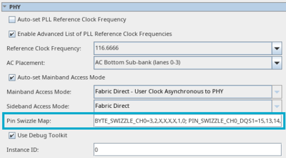
Pin Swizzle Map
The Quartus® Prime software uses fixed pin placement for each supported memory standard, as described in the Pin Placement topic in the Architecture chapter. Do not make changes using a .qsf assignment or the pin planner if you need to swap the DQ pins within a DQS group or the DQS group within a channel/interface. Fitter errors may occur if you enter the incorrect pin location for the EMIF interface. The following is an example of a fitter error for LPDDR4 protocol when an incorrect pin assignment is specified:
Error (175001): The Fitter cannot place 1 BYTE, which is within Generic Component ed_synth_emif_io96b_lpddr4_0.
The Pin Swizzle Map allows you to specify the ordering of the physical connections of each DQ pin on the memory component to the FPGA. Incorrect information entered in the Pin Swizzle Map may cause calibration errors.
Refer to Configuring DQ Pin Swizzling for information on configuring DQ pin swizzling.
Pin Swizzle Map for Component interfaces
For component interfaces, you must match the net name in the schematic to the index of default pin placement, to determine the pin swizzling specification.
Consider the example of DQS Group 0 for Channel 1 on the LPDDR4 Component interface, as shown in the table below:
| Lane | Pin Index | Default Pin Placement | Net Name in Schematic | Swizzling Index |
|---|---|---|---|---|
| BL6 | 83 | MEM_0_MEM_DQ [23] | MEM_1_MEM_DQ [11] | 11 |
| 82 | MEM_0_MEM_DQ [22] | MEM_1_MEM_DQ [10] | 10 | |
| 81 | MEM_0_MEM_DQ [21] | MEM_1_MEM_DQ [8] | 8 | |
| 80 | MEM_0_MEM_DQ [20] | MEM_1_MEM_DQ [9] | 9 | |
| 79 | ||||
| 78 | MEM_0_MEM_DMI [2] | MEM_0_MEM_DMI [1] | ||
| 77 | MEM_0_MEM_DQS_C [2] | MEM_0_MEM_DQS_C [1] | ||
| 76 | MEM_0_MEM_DQS_T [2] | MEM_0_MEM_DQS_T [1] | ||
| 75 | MEM_0_MEM_DQ [19] | MEM_1_MEM_DQ [12] | 12 | |
| 74 | MEM_0_MEM_DQ [18] | MEM_1_MEM_DQ [14] | 14 | |
| 73 | MEM_0_MEM_DQ [17] | MEM_1_MEM_DQ [13] | 13 | |
| 72 | MEM_0_MEM_DQ [16] | MEM_1_MEM_DQ [15] | 15 |
For this specific group, the correct pin swizzling specification is:
PIN_SWIZZLE_CH0_DQS1 = 15,13,14,12,9,8,10,11;
The following example shows pin swizzle map parameters. You must add all parameters to the pin swizzle map in a single line, each separated by semi-colons as shown:
BYTE_SWIZZLE_CH0=3,2,X,X,X,X,1,0;
PIN_SWIZZLE_CH0_DQS1=15,13,14,12,9,8,10,11;
PIN_SWIZZLE_CH0_DQS0=3,2,1,0,5,4,7,6;
PIN_SWIZZLE_CH0_DQS3=31,30,28,29,25,24,26,27;
PIN_SWIZZLE_CH0_DQS2= 16,18,17,19,23,20,22,21;