External Memory Interfaces (EMIF) IP User Guide: Agilex™ 3 FPGAs and SoCs
ID
847458
Date
4/24/2025
Public
A newer version of this document is available. Customers should click here to go to the newest version.
1. About the External Memory Interfaces Agilex™ 3 FPGA IP
2. Agilex™ 3 FPGA EMIF IP – Introduction
3. Agilex™ 3 FPGA EMIF IP - Configuring and Generating the IP
4. Agilex™ 3 FPGA EMIF IP – Simulating Memory IP
5. Agilex™ 3 FPGA EMIF IP - Validating the IP
6. Agilex 3 FPGA EMIF IP Debugging
7. Document Revision History for External Memory Interfaces (EMIF) IP User Guide
A. Agilex™ 3 FPGA EMIF IP – Product Architecture
B. Agilex™ 3 FPGA EMIF IP – End-User Signals
3.1. Creating an EMIF Project
3.2. Generating and Configuring the EMIF IP
3.3. EMIF IP LPDDR4 Parameter Descriptions
3.4. Generating HDL for Synthesis and Simulation
3.5. Generating the Synthesizable EMIF Design Example
3.6. Agilex™ 3 FPGA EMIF IP Pin and Resource Planning
3.7. Compiling the Agilex™ 3 EMIF Design Example
3.8. Agilex™ 3 FPGA EMIF IP – Timing Closure
3.9. Agilex™ 3 FPGA EMIF IP – Controller Optimization
3.3.1.1. Example: DQ Pin Swizzling Within DQS Group for a x32 LPDDR4 Interface
3.3.1.2. Example: Byte Swizzling for x32 LPDDR4 Interface
3.3.1.3. Example: Combining Pin and Byte Swizzling
3.3.1.4. Example: DQ Pin Swizzling Within DQS Group for 2 Channel x16 LPDDR4 Interface
3.3.1.5. Example: Byte Swizzling for 2 Channel x16 LPDDR4 Interface
6.1. Interface Configuration Performance Issues
6.2. Functional Issue Evaluation
6.3. Timing Issue Characteristics
6.4. Evaluating FPGA Timing Issues
6.5. Verifying Memory IP Using the Signal Tap Logic Analyzer
6.6. Guidelines for Developing HDL for Traffic Generator
6.7. Debugging with the External Memory Interface Debug Toolkit
6.8. Guidelines for Traffic Generator Status Check
6.9. Hardware Debugging Guidelines
6.10. Categorizing Hardware Issues
6.11. Agilex™ 3 FPGA EMIF IP - Mailbox Support
6.9.1. Create a Simplified Design that Demonstrates the Same Issue
6.9.2. Measure Power Distribution Network
6.9.3. Measure Signal Integrity and Setup and Hold Margin
6.9.4. Vary Voltage
6.9.5. Operate at a Lower Speed
6.9.6. Determine Whether the Issue Exists in Previous Versions of Software
6.9.7. Determine Whether the Issue Exists in the Current Version of Software
6.9.8. Try A Different PCB
6.9.9. Try Other Configurations
6.9.10. Debugging Checklist
6.10.1.1. Characteristics of Signal Integrity Issues
6.10.1.2. Evaluating Signal Integrity Issues
6.10.1.3. Skew
6.10.1.4. Crosstalk
6.10.1.5. Power System
6.10.1.6. Clock Signals
6.10.1.7. Address and Command Signals
6.10.1.8. Read Data Valid Window and Eye Diagram
6.10.1.9. Write Data Valid Window and Eye Diagram
A.1.1. Agilex™ 3 EMIF Architecture: I/O Subsystem
A.1.2. Agilex™ 3 EMIF Architecture: I/O SSM
A.1.3. Agilex™ 3 EMIF Architecture: HSIO Bank
A.1.4. Agilex™ 3 EMIF Architecture: I/O Lane
A.1.5. Agilex™ 3 EMIF Architecture: Input DQS Clock Tree
A.1.6. Agilex™ 3 EMIF Architecture: PHY Clock Tree
A.1.7. Agilex™ 3 EMIF Architecture: PLL Reference Clock Networks
A.1.8. Agilex™ 3 EMIF Architecture: Clock Phase Alignment
A.1.9. User Clock in Different Core Access Modes
A.1.10. Agilex™ 3 EMIF Sequencer
A.1.11. Agilex™ 3 EMIF Controller
A.1.12. Hard Memory Controller
A.1.13. Agilex™ 3 EMIF IP for Hard Processor Subsystem (HPS)
B.1. IP Interfaces for External Memory Interfaces (EMIF) IP - LPDDR4
B.2. s0_axi4_clock_in for External Memory Interfaces (EMIF) IP - LPDDR4
B.3. core_init_n for External Memory Interfaces (EMIF) IP - LPDDR4
B.4. s0_axi4_clock_in for External Memory Interfaces (EMIF) IP - LPDDR4
B.5. core_init_n for External Memory Interfaces (EMIF) IP - LPDDR4
B.6. s0_axi4_ctrl_ready for External Memory Interfaces (EMIF) IP - LPDDR4
B.7. s0_axi4_clock_out for External Memory Interfaces (EMIF) IP - LPDDR4
B.8. s1_axi4_ctrl_ready for External Memory Interfaces (EMIF) IP - LPDDR4
B.9. s0_axi4 for External Memory Interfaces (EMIF) IP - LPDDR4
B.10. s1_axi4 for External Memory Interfaces (EMIF) IP - LPDDR4
B.11. io96b0_to_hps for External Memory Interfaces (EMIF) IP - LPDDR4
B.12. io96b1_to_hps for External Memory Interfaces (EMIF) IP - LPDDR4
B.13. s0_axi4lite_clock for External Memory Interfaces (EMIF) IP - LPDDR4
B.14. s0_axi4lite_reset_n for External Memory Interfaces (EMIF) IP - LPDDR4
B.15. s0_axi4lite for External Memory Interfaces (EMIF) IP - LPDDR4
B.16. mem_0 for External Memory Interfaces (EMIF) IP - LPDDR4
B.17. mem_ck_0 for External Memory Interfaces (EMIF) IP - LPDDR4
B.18. mem_1 for External Memory Interfaces (EMIF) IP - LPDDR4
B.19. mem_ck_1 for External Memory Interfaces (EMIF) IP - LPDDR4
B.20. mem_reset_n for External Memory Interfaces (EMIF) IP - LPDDR4
B.21. oct_0 for External Memory Interfaces (EMIF) IP - LPDDR4
B.22. oct_1 for External Memory Interfaces (EMIF) IP - LPDDR4
B.23. ref_clk for External Memory Interfaces (EMIF) IP - LPDDR4
3.5. Generating the Synthesizable EMIF Design Example
The Agilex™ 3 development kit is designed for an LPDDR4 x32 interface. For designs targeting the development kit, you set the High-level Configuration tab to match your hardware implementation. To generate the synthesizable design example, follow these steps:
- On the Example Design tab, ensure that the Synthesis box is set as True.
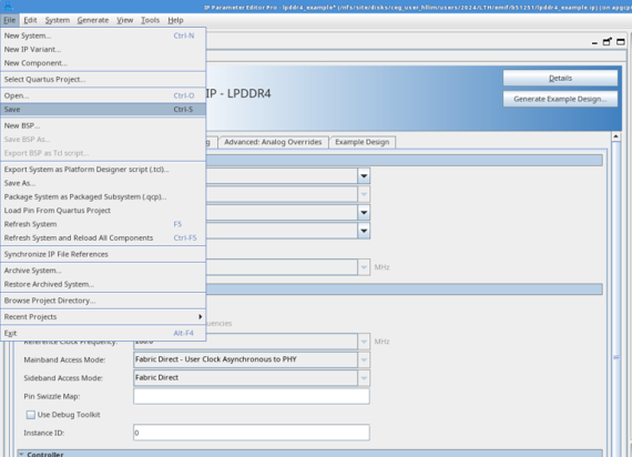
- If you are implementing a single interface example design, configure the EMIF IP and click File > Save to save the current settings into the IP variation file (<user instance name>.ip).
Figure 18. Saving the Current Settings
- If you are implementing a single interface example design, configure the EMIF IP and click File > Save to save the current settings into the IP variation file (<user instance name>.ip).
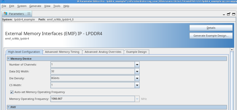
- Click Generate Example Design in the upper-right corner of the window.
Figure 19. Generate Example Design
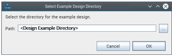
- Specify a directory for the EMIF design example and click OK. Successful generation of the EMIF design example creates the synthesis file set under a qii directory.
Figure 20. Specifying a Directory
- Click File > Exit to exit the IP Parameter Editor Pro window. The system prompts, Recent changes have not been generated. Generate now? Click No to continue with the next flow.
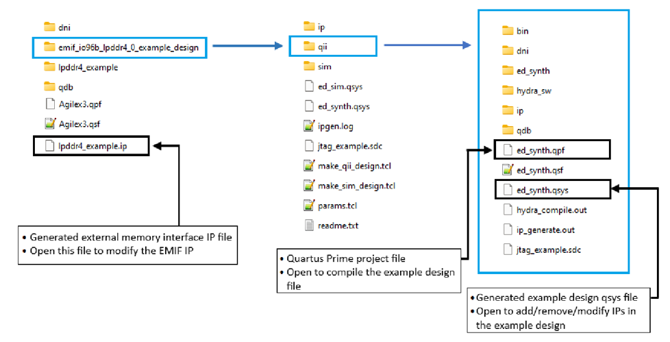
- To open the example design, click File > Open Project, and navigate to the <project_directory>/<design_example_name>/qii/ed_synth.qpf and click Open.
Note: For information on compiling the design example, refer to Compiling the EMIF Design Example .Figure 21. Generated Synthesizable Design Example File Structure
Note:
- For information on debugging, refer to Configuring a Design to Use the Debug Toolkit.
- If you don't specify Simulation or Synthesis from the dropdown menu, the destination directory contains only Platform Designer design files, which the Quartus® Prime software cannot compile directly, but which you can view or edit in the Platform Designer. In this situation you can run the following commands to generate synthesis and simulation file sets:
- To create an Quartus® Prime software-compilable project, run the
quartus_sh -t make_qii_design.tcl
script in the destination directory. - To create a simulation project, run the
quartus_sh -t make_sim_design.tcl
script in the destination directory.
- To create an Quartus® Prime software-compilable project, run the
- If you have generated a design example and then make changes to it in the parameter editor, you must regenerate the design example to see your changes implemented. The newly generated design example does not overwrite the existing design example files.