External Memory Interfaces (EMIF) IP User Guide: Agilex™ 3 FPGAs and SoCs
ID
847458
Date
4/24/2025
Public
A newer version of this document is available. Customers should click here to go to the newest version.
1. About the External Memory Interfaces Agilex™ 3 FPGA IP
2. Agilex™ 3 FPGA EMIF IP – Introduction
3. Agilex™ 3 FPGA EMIF IP - Configuring and Generating the IP
4. Agilex™ 3 FPGA EMIF IP – Simulating Memory IP
5. Agilex™ 3 FPGA EMIF IP - Validating the IP
6. Agilex 3 FPGA EMIF IP Debugging
7. Document Revision History for External Memory Interfaces (EMIF) IP User Guide
A. Agilex™ 3 FPGA EMIF IP – Product Architecture
B. Agilex™ 3 FPGA EMIF IP – End-User Signals
3.1. Creating an EMIF Project
3.2. Generating and Configuring the EMIF IP
3.3. EMIF IP LPDDR4 Parameter Descriptions
3.4. Generating HDL for Synthesis and Simulation
3.5. Generating the Synthesizable EMIF Design Example
3.6. Agilex™ 3 FPGA EMIF IP Pin and Resource Planning
3.7. Compiling the Agilex™ 3 EMIF Design Example
3.8. Agilex™ 3 FPGA EMIF IP – Timing Closure
3.9. Agilex™ 3 FPGA EMIF IP – Controller Optimization
3.3.1.1. Example: DQ Pin Swizzling Within DQS Group for a x32 LPDDR4 Interface
3.3.1.2. Example: Byte Swizzling for x32 LPDDR4 Interface
3.3.1.3. Example: Combining Pin and Byte Swizzling
3.3.1.4. Example: DQ Pin Swizzling Within DQS Group for 2 Channel x16 LPDDR4 Interface
3.3.1.5. Example: Byte Swizzling for 2 Channel x16 LPDDR4 Interface
6.1. Interface Configuration Performance Issues
6.2. Functional Issue Evaluation
6.3. Timing Issue Characteristics
6.4. Evaluating FPGA Timing Issues
6.5. Verifying Memory IP Using the Signal Tap Logic Analyzer
6.6. Guidelines for Developing HDL for Traffic Generator
6.7. Debugging with the External Memory Interface Debug Toolkit
6.8. Guidelines for Traffic Generator Status Check
6.9. Hardware Debugging Guidelines
6.10. Categorizing Hardware Issues
6.11. Agilex™ 3 FPGA EMIF IP - Mailbox Support
6.9.1. Create a Simplified Design that Demonstrates the Same Issue
6.9.2. Measure Power Distribution Network
6.9.3. Measure Signal Integrity and Setup and Hold Margin
6.9.4. Vary Voltage
6.9.5. Operate at a Lower Speed
6.9.6. Determine Whether the Issue Exists in Previous Versions of Software
6.9.7. Determine Whether the Issue Exists in the Current Version of Software
6.9.8. Try A Different PCB
6.9.9. Try Other Configurations
6.9.10. Debugging Checklist
6.10.1.1. Characteristics of Signal Integrity Issues
6.10.1.2. Evaluating Signal Integrity Issues
6.10.1.3. Skew
6.10.1.4. Crosstalk
6.10.1.5. Power System
6.10.1.6. Clock Signals
6.10.1.7. Address and Command Signals
6.10.1.8. Read Data Valid Window and Eye Diagram
6.10.1.9. Write Data Valid Window and Eye Diagram
A.1.1. Agilex™ 3 EMIF Architecture: I/O Subsystem
A.1.2. Agilex™ 3 EMIF Architecture: I/O SSM
A.1.3. Agilex™ 3 EMIF Architecture: HSIO Bank
A.1.4. Agilex™ 3 EMIF Architecture: I/O Lane
A.1.5. Agilex™ 3 EMIF Architecture: Input DQS Clock Tree
A.1.6. Agilex™ 3 EMIF Architecture: PHY Clock Tree
A.1.7. Agilex™ 3 EMIF Architecture: PLL Reference Clock Networks
A.1.8. Agilex™ 3 EMIF Architecture: Clock Phase Alignment
A.1.9. User Clock in Different Core Access Modes
A.1.10. Agilex™ 3 EMIF Sequencer
A.1.11. Agilex™ 3 EMIF Controller
A.1.12. Hard Memory Controller
A.1.13. Agilex™ 3 EMIF IP for Hard Processor Subsystem (HPS)
B.1. IP Interfaces for External Memory Interfaces (EMIF) IP - LPDDR4
B.2. s0_axi4_clock_in for External Memory Interfaces (EMIF) IP - LPDDR4
B.3. core_init_n for External Memory Interfaces (EMIF) IP - LPDDR4
B.4. s0_axi4_clock_in for External Memory Interfaces (EMIF) IP - LPDDR4
B.5. core_init_n for External Memory Interfaces (EMIF) IP - LPDDR4
B.6. s0_axi4_ctrl_ready for External Memory Interfaces (EMIF) IP - LPDDR4
B.7. s0_axi4_clock_out for External Memory Interfaces (EMIF) IP - LPDDR4
B.8. s1_axi4_ctrl_ready for External Memory Interfaces (EMIF) IP - LPDDR4
B.9. s0_axi4 for External Memory Interfaces (EMIF) IP - LPDDR4
B.10. s1_axi4 for External Memory Interfaces (EMIF) IP - LPDDR4
B.11. io96b0_to_hps for External Memory Interfaces (EMIF) IP - LPDDR4
B.12. io96b1_to_hps for External Memory Interfaces (EMIF) IP - LPDDR4
B.13. s0_axi4lite_clock for External Memory Interfaces (EMIF) IP - LPDDR4
B.14. s0_axi4lite_reset_n for External Memory Interfaces (EMIF) IP - LPDDR4
B.15. s0_axi4lite for External Memory Interfaces (EMIF) IP - LPDDR4
B.16. mem_0 for External Memory Interfaces (EMIF) IP - LPDDR4
B.17. mem_ck_0 for External Memory Interfaces (EMIF) IP - LPDDR4
B.18. mem_1 for External Memory Interfaces (EMIF) IP - LPDDR4
B.19. mem_ck_1 for External Memory Interfaces (EMIF) IP - LPDDR4
B.20. mem_reset_n for External Memory Interfaces (EMIF) IP - LPDDR4
B.21. oct_0 for External Memory Interfaces (EMIF) IP - LPDDR4
B.22. oct_1 for External Memory Interfaces (EMIF) IP - LPDDR4
B.23. ref_clk for External Memory Interfaces (EMIF) IP - LPDDR4
6.8.2. Exporting the Status Interface to the Top-Level Design
Do not perform this procedure if you plan to observe signal activity through the Signal Tap Logic Analyzer only.
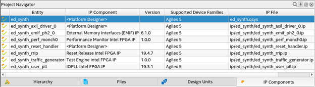
Using the Agilex™ 3 FPGA EMIF IP design example, perform the following steps to export the traffic generator traffic signals:
- Navigate to the IP Components tab in the Project Navigator, and click ed_synth.qsys to open the design in the Platform Designer.
Figure 41.
- Click on Test Engine Intel FPGA IP and go to the Remote Access tab.
- Check the Export status interface box.
- Note the status port available in the IP instance. Export the status signal to the top-level design.
Figure 42.

- Save the design.
- Click Sync System Infos and Generate HDL.
Figure 43.

- Compile the design. You can observe the status_status_done and status_status_error signals exported at the top level of the traffic_generator instance.
Figure 44.
