External Memory Interfaces (EMIF) IP User Guide: Agilex™ 3 FPGAs and SoCs
ID
847458
Date
4/24/2025
Public
A newer version of this document is available. Customers should click here to go to the newest version.
1. About the External Memory Interfaces Agilex™ 3 FPGA IP
2. Agilex™ 3 FPGA EMIF IP – Introduction
3. Agilex™ 3 FPGA EMIF IP - Configuring and Generating the IP
4. Agilex™ 3 FPGA EMIF IP – Simulating Memory IP
5. Agilex™ 3 FPGA EMIF IP - Validating the IP
6. Agilex 3 FPGA EMIF IP Debugging
7. Document Revision History for External Memory Interfaces (EMIF) IP User Guide
A. Agilex™ 3 FPGA EMIF IP – Product Architecture
B. Agilex™ 3 FPGA EMIF IP – End-User Signals
3.1. Creating an EMIF Project
3.2. Generating and Configuring the EMIF IP
3.3. EMIF IP LPDDR4 Parameter Descriptions
3.4. Generating HDL for Synthesis and Simulation
3.5. Generating the Synthesizable EMIF Design Example
3.6. Agilex™ 3 FPGA EMIF IP Pin and Resource Planning
3.7. Compiling the Agilex™ 3 EMIF Design Example
3.8. Agilex™ 3 FPGA EMIF IP – Timing Closure
3.9. Agilex™ 3 FPGA EMIF IP – Controller Optimization
3.3.1.1. Example: DQ Pin Swizzling Within DQS Group for a x32 LPDDR4 Interface
3.3.1.2. Example: Byte Swizzling for x32 LPDDR4 Interface
3.3.1.3. Example: Combining Pin and Byte Swizzling
3.3.1.4. Example: DQ Pin Swizzling Within DQS Group for 2 Channel x16 LPDDR4 Interface
3.3.1.5. Example: Byte Swizzling for 2 Channel x16 LPDDR4 Interface
6.1. Interface Configuration Performance Issues
6.2. Functional Issue Evaluation
6.3. Timing Issue Characteristics
6.4. Evaluating FPGA Timing Issues
6.5. Verifying Memory IP Using the Signal Tap Logic Analyzer
6.6. Guidelines for Developing HDL for Traffic Generator
6.7. Debugging with the External Memory Interface Debug Toolkit
6.8. Guidelines for Traffic Generator Status Check
6.9. Hardware Debugging Guidelines
6.10. Categorizing Hardware Issues
6.11. Agilex™ 3 FPGA EMIF IP - Mailbox Support
6.9.1. Create a Simplified Design that Demonstrates the Same Issue
6.9.2. Measure Power Distribution Network
6.9.3. Measure Signal Integrity and Setup and Hold Margin
6.9.4. Vary Voltage
6.9.5. Operate at a Lower Speed
6.9.6. Determine Whether the Issue Exists in Previous Versions of Software
6.9.7. Determine Whether the Issue Exists in the Current Version of Software
6.9.8. Try A Different PCB
6.9.9. Try Other Configurations
6.9.10. Debugging Checklist
6.10.1.1. Characteristics of Signal Integrity Issues
6.10.1.2. Evaluating Signal Integrity Issues
6.10.1.3. Skew
6.10.1.4. Crosstalk
6.10.1.5. Power System
6.10.1.6. Clock Signals
6.10.1.7. Address and Command Signals
6.10.1.8. Read Data Valid Window and Eye Diagram
6.10.1.9. Write Data Valid Window and Eye Diagram
A.1.1. Agilex™ 3 EMIF Architecture: I/O Subsystem
A.1.2. Agilex™ 3 EMIF Architecture: I/O SSM
A.1.3. Agilex™ 3 EMIF Architecture: HSIO Bank
A.1.4. Agilex™ 3 EMIF Architecture: I/O Lane
A.1.5. Agilex™ 3 EMIF Architecture: Input DQS Clock Tree
A.1.6. Agilex™ 3 EMIF Architecture: PHY Clock Tree
A.1.7. Agilex™ 3 EMIF Architecture: PLL Reference Clock Networks
A.1.8. Agilex™ 3 EMIF Architecture: Clock Phase Alignment
A.1.9. User Clock in Different Core Access Modes
A.1.10. Agilex™ 3 EMIF Sequencer
A.1.11. Agilex™ 3 EMIF Controller
A.1.12. Hard Memory Controller
A.1.13. Agilex™ 3 EMIF IP for Hard Processor Subsystem (HPS)
B.1. IP Interfaces for External Memory Interfaces (EMIF) IP - LPDDR4
B.2. s0_axi4_clock_in for External Memory Interfaces (EMIF) IP - LPDDR4
B.3. core_init_n for External Memory Interfaces (EMIF) IP - LPDDR4
B.4. s0_axi4_clock_in for External Memory Interfaces (EMIF) IP - LPDDR4
B.5. core_init_n for External Memory Interfaces (EMIF) IP - LPDDR4
B.6. s0_axi4_ctrl_ready for External Memory Interfaces (EMIF) IP - LPDDR4
B.7. s0_axi4_clock_out for External Memory Interfaces (EMIF) IP - LPDDR4
B.8. s1_axi4_ctrl_ready for External Memory Interfaces (EMIF) IP - LPDDR4
B.9. s0_axi4 for External Memory Interfaces (EMIF) IP - LPDDR4
B.10. s1_axi4 for External Memory Interfaces (EMIF) IP - LPDDR4
B.11. io96b0_to_hps for External Memory Interfaces (EMIF) IP - LPDDR4
B.12. io96b1_to_hps for External Memory Interfaces (EMIF) IP - LPDDR4
B.13. s0_axi4lite_clock for External Memory Interfaces (EMIF) IP - LPDDR4
B.14. s0_axi4lite_reset_n for External Memory Interfaces (EMIF) IP - LPDDR4
B.15. s0_axi4lite for External Memory Interfaces (EMIF) IP - LPDDR4
B.16. mem_0 for External Memory Interfaces (EMIF) IP - LPDDR4
B.17. mem_ck_0 for External Memory Interfaces (EMIF) IP - LPDDR4
B.18. mem_1 for External Memory Interfaces (EMIF) IP - LPDDR4
B.19. mem_ck_1 for External Memory Interfaces (EMIF) IP - LPDDR4
B.20. mem_reset_n for External Memory Interfaces (EMIF) IP - LPDDR4
B.21. oct_0 for External Memory Interfaces (EMIF) IP - LPDDR4
B.22. oct_1 for External Memory Interfaces (EMIF) IP - LPDDR4
B.23. ref_clk for External Memory Interfaces (EMIF) IP - LPDDR4
5.2. Checking the EMIF Design Example with the Performance Monitor
You can use the Performance Monitor (PMON) to check the performance metrics of the EMIF interface.
The Performance Monitor is a synthesizable block consisting of control and status registers that let you configure and modify the performance metrics of the EMIF Interface. The Performance Monitor allows you to measure the following performance metrics:
- Read latency
- Write latency
- Read efficiency
- Write efficiency
- Overall efficiency
- Subchannel efficiency
- Subchannel back pressure
- Expected transactions in subchannel
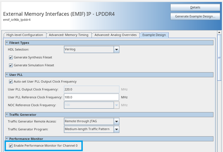
Figure 33. Enabling the Performance Monitor in the EMIF IP
Note: Do not run any traffic on the interface that PMON is monitoring, while you are configuring PMON. Failure to observe this restriction can result in inaccurate measurements.
To generate a design example with the Performance Monitor, follow these steps:
- When generating your design example, set the Enable Performance Monitor parameter to True. This includes the Performance Monitor FPGA IP, which allows you to measure performance on an AIX4 mainband interface.
- Open the generated design example and navigate to the Quartus® Prime Pro Edition software folder containing the design example directory:
<project_directory>/<example_design_directory>/qii/ed_synth.qpf
- Make the necessary pin assignments in the .qsf file or by using the Pin Planner and compile the design by clicking Processing > Start Compilation. This generates a .sof file, which you can configure into hardware.
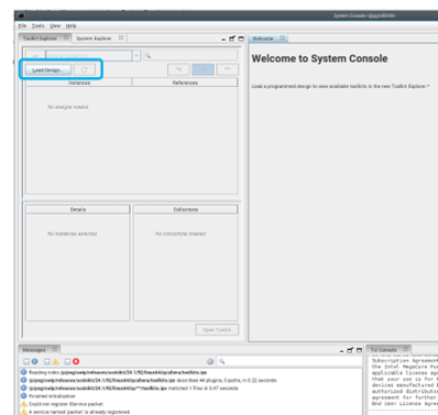
- Open the System Console from the Quartus® Prime Pro Edition software by clicking Load Design.
Figure 34. Load Design
- Load the pmon_library.tcl file in the system console by typing the following command:
source pmon_library.tcl
- Load the testengine_library.tcl file in the system console by typing the following command:
source testengine_library.tcl
- Set the metric configuration on desired AXI4 performance monitors:
- To monitor the read latency only:
pmon_set_all basic_ro
- To monitor the write latency only:
pmon_set_all basic_wo
- To monitor read and write latency only:
pmon_set_all basic_rw
- To monitor read latency, write latency, average number of transactions per cycle:
pmon_set_all basic_eff
- For more information on the configurations that you can monitor, use the following command to access to all the metric configurations:
pmon_help config
- To monitor the read latency only:
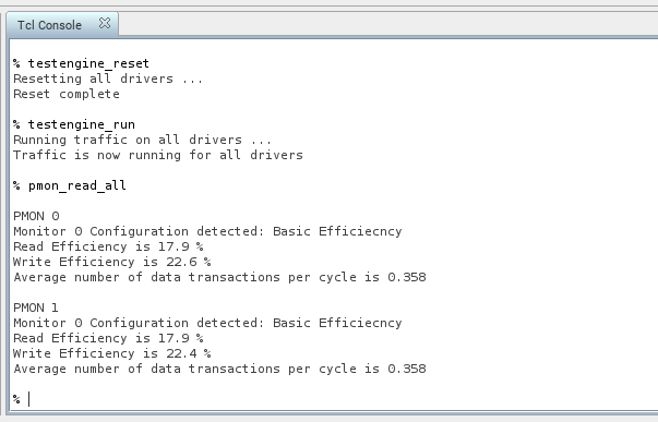
- Clear the counters and internal state of all performance monitors by typing the following command:
pmon_reset_counter_data_all
- Reset the state of the drivers by typing the following command:
testengine_reset
- Run traffic over the interface by typing the following command:
testengine_run
- Read the efficiency metrics on the AXI4 performance monitor by typing:
pmon_read_all
Successful reading of performance metrics produces results similar to that shown below:Figure 35. Performance Monitor (PMON) Results