Intel Agilex® 7 General-Purpose I/O User Guide: M-Series
ID
772138
Date
9/11/2023
Public
A newer version of this document is available. Customers should click here to go to the newest version.
1. Intel Agilex® 7 M-Series General-Purpose I/O Overview
2. Intel Agilex® 7 M-Series GPIO-B Banks
3. Intel Agilex® 7 M-Series HPS I/O Banks
4. Intel Agilex® 7 M-Series SDM I/O Banks
5. Intel Agilex® 7 M-Series I/O Troubleshooting Guidelines
6. GPIO Intel® FPGA IP
7. Programmable I/O Features Description
8. Documentation Related to the Intel Agilex® 7 General-Purpose I/O User Guide: M-Series
9. Document Revision History for the Intel Agilex® 7 General-Purpose I/O User Guide: M-Series
2.5.1. I/O Standard Placement Restrictions for True Differential I/Os
2.5.2. Placement Restrictions for True Differential and Single-Ended I/O Standards in the Same or Adjacent GPIO-B Bank
2.5.3. VREF Sources and Input Standards Grouping
2.5.4. GPIO-B Pin Restrictions for External Memory Interfaces
2.5.5. RZQ Pin Requirement
2.5.6. I/O Standards Implementation Based on VCCIO_PIO Voltages
2.5.7. I/O Standard Selection and I/O Bank Supply Compatibility Check
2.5.8. Simultaneous Switching Noise
2.5.9. HPS Shared I/O Requirements
2.5.10. Clocking Requirements
2.5.11. SDM Shared I/O Requirements
2.5.12. Unused Pins
2.5.13. VCCIO_PIO Supply for Unused GPIO-B Banks
2.5.14. GPIO-B Pins During Power Sequencing
2.5.15. Drive Strength Requirement for GPIO-B Input Pins
2.5.16. Maximum DC Current Restrictions
2.5.17. 1.05 V, 1.1 V, or 1.2 V I/O Interface Voltage Level Compatibility
2.5.18. Connection to True Differential Signaling Input Buffers During Device Reconfiguration
2.5.19. LVSTL700 I/O Standards Differential Pin Pair Requirements
2.5.20. Implementing a Pseudo Open Drain
2.5.21. Allowed Duration for Using RT OCT
2.5.22. Single-Ended Strobe Signal Differential Pin Pair Restriction
6.1. Release Information for GPIO Intel® FPGA IP
6.2. Generating the GPIO Intel® FPGA IP
6.3. GPIO Intel® FPGA IP Parameter Settings
6.4. GPIO Intel® FPGA IP Interface Signals
6.5. GPIO Intel® FPGA IP Architecture
6.6. Verifying Resource Utilization and Design Performance
6.7. GPIO Intel® FPGA IP Timing
6.8. GPIO Intel® FPGA IP Design Examples
3.3.2. I/O Assignments with the Intel® Quartus® Prime Assignment Editor
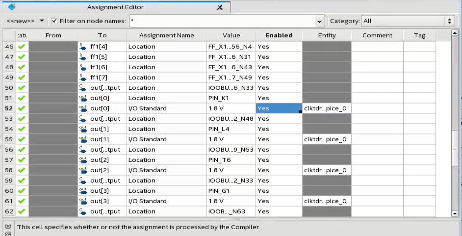
You can assign all instance-specific settings and constraints through the Intel® Quartus® Prime Assignment Editor. You can filter assignments by node name or category.
Figure 26. Intel® Quartus® Prime Assignment Editor This figure shows an example of the user interface and does not represent actual components, features, or settings supported by M-Series FPGAs.

