A newer version of this document is available. Customers should click here to go to the newest version.
1. FPGA AI Suite SoC Design Example User Guide
2. About the SoC Design Example
3. FPGA AI Suite SoC Design Example Quick Start Tutorial
4. FPGA AI Suite SoC Design Example Run Process
5. FPGA AI Suite SoC Design Example Build Process
6. FPGA AI Suite SoC Design Example Quartus® Prime System Architecture
7. FPGA AI Suite Soc Design Example Software Components
8. Streaming-to-Memory (S2M) Streaming Demonstration
A. FPGA AI Suite SoC Design Example User Guide Archives
B. FPGA AI Suite SoC Design Example User Guide Document Revision History
3.1. Initial Setup
3.2. Initializing a Work Directory
3.3. (Optional) Create an SD Card Image (.wic)
3.4. Writing the SD Card Image (.wic) to an SD Card
3.5. Preparing SoC FPGA Development Kits for the FPGA AI Suite SoC Design Example
3.6. Adding Compiled Graphs (AOT files) to the SD Card
3.7. Verifying FPGA Device Drivers
3.8. Running the Demonstration Applications
7.1.1. Yocto Recipe: recipes-core/images/coredla-image.bb
7.1.2. Yocto Recipe: recipes-bsp/u-boot/u-boot-socfpga_%.bbappend
7.1.3. Yocto Recipe: recipes-drivers/msgdma-userio/msgdma-userio.bb
7.1.4. Yocto Recipe: recipes-drivers/uio-devices/uio-devices.bb
7.1.5. Yocto Recipe: recipes-kernel/linux/linux-socfpga-lts_5.15.bbappend
7.1.6. Yocto Recipe: wic
6.5. The SoC Design Example Platform Designer System
At the center of the SoC design example is the Platform Designer system.
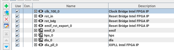
In Platform Designer, the SoC design example is separated into three hierarchical layers, the:
- emif_0 : This layer contains the FPGA DDR4 External Memory Interface
- dla_0 : This layer contains all the DLA IP and infrastructure IP
- hps_0 : This layer contains all the ARM-HPS, ARM-EMIF and infrastructure IP for the ARM
The division of hierarchy demonstrates the sections of the design that are relevant to the solution. For example, if you want to target another board with a different external memory interface, you need to edit only the emif_0 layer.