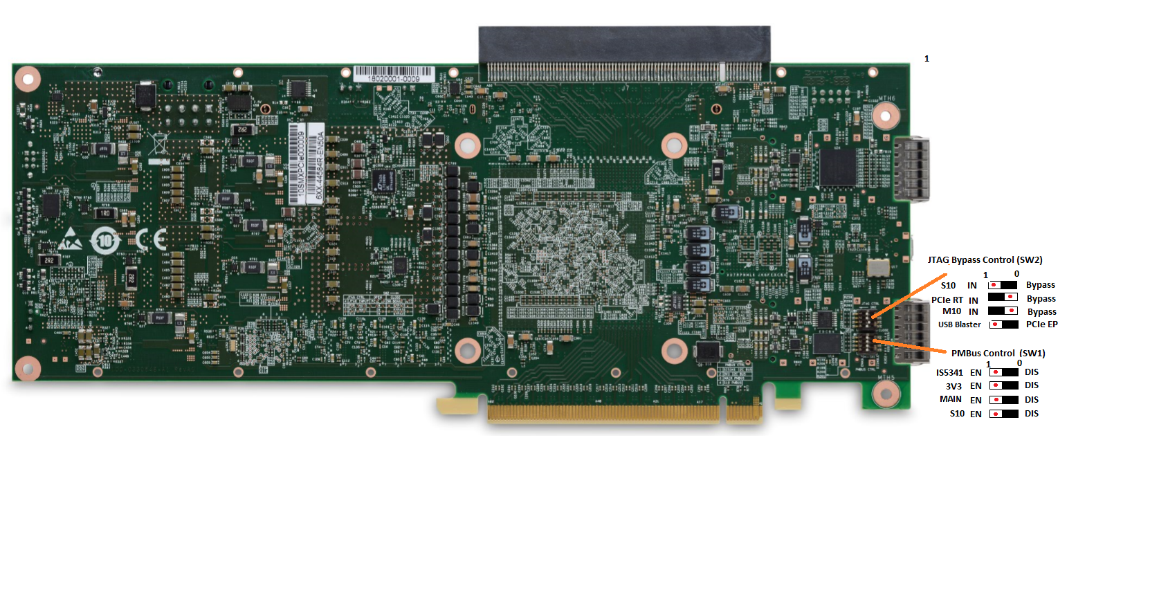
3.2. Default Switch and Jumper Settings
Figure 3. Default Switch Settings
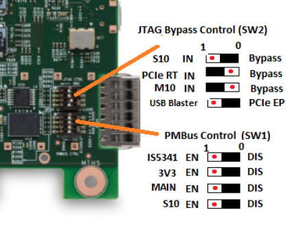
| Switch | Board Label | Function | Default Position |
|---|---|---|---|
| 1 | JTAG INPUT | JTAG Source Select |
OFF (On-board Intel® FPGA Download Cable) |
| 2 | M10 | MAX® 10 JTAG |
ON (JTAG OUT) |
| 3 | PCIE RT | PCIe* Root Port JTAG |
ON (JTAG OUT) |
| 4 | S10 | Stratix® 10 FPGA JTAG |
OFF (JTAG IN) |
| Switch | Board Label | Function | Default Position |
|---|---|---|---|
| 1 | SI5341 I2C BUS | Clock Generator I2C Bus | OFF (Enable) |
| 2 | 3V3 I2C BUS | 3V3 VRM I2C BUS | OFF (Enable) |
| 3 | MAIN I2C BUS | MAIN I2C BUS | OFF (Enable) |
| 4 | S10 PMBus | Stratix® 10 FPGA PMBus | OFF (Enable) |