AN 672: Transceiver Link Design Guidelines for High-Gbps Data Rate Transmission
1.1.4. Copper Surface Roughness
In addition to dielectric loss, material losses also result from conductor loss. Conductor loss is the resistive attenuation on the copper conductor. Resistive loss is usually mitigated by using appropriately wide traces. However, for very high frequency designs, the majority of the current distribution is pushed towards the outer surface of the copper conductor as a result of the skin effect. At frequencies where the skin depth approaches the average roughness of the copper, the current flow is further impeded by the copper surface roughness, causing increased resistance and conductor loss.
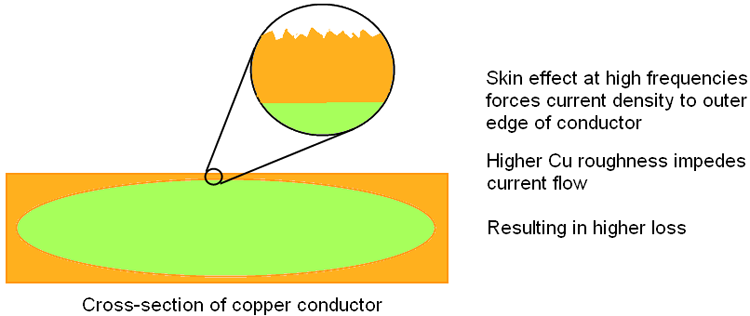
The roughness of the copper surface varies depending on the construction of the copper foils. These foils are either electrodeposited (commonly referred to as ED copper) or rolled and pressed to create a smoother copper foil surface. The copper roughness is specified as an average value (Ra) in micrometers (µm). As a comparison, typical ED copper roughness has Ra of 1 µm or more while rolled copper ranges from 0.3 to 0.4 µm. The effect of this copper roughness can be approximated by a correction factor (KSR) to the attenuation of the conductor (αCond).
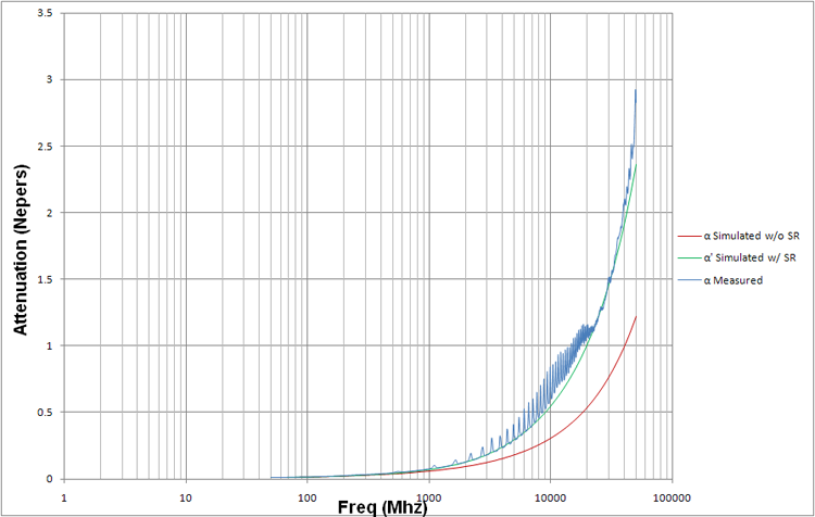
The red curve is the high frequency structural simulator (HFSS) simulated attenuation of the conductor (αCond ) without the effects of surface roughness correction. The green curve is the same result with the surface roughness correction factor (KSR) included. The blue curve is the actual vector network analyzer (VNA) measurement of the same test trace for correlation purposes.