1.3.6. Blocking Cap Optimization
Transceiver channels often incorporate DC blocking capacitors to control the common mode voltage at the receiver. However, the presence of the blocking capacitors in the channel creates an abrupt discontinuity where the trace meets the capacitor. Similar to via optimization, the layout footprint for the blocking caps can be optimized to minimize their impact on the channel. Because the larger capacitor pad results in lowering its characteristic impedance, one way of increasing this impedance to better match the trace impedance is to increase the distance to the reference by making cut-outs underneath the body of the capacitor footprint.
By cutting out the first reference plane directly below the capacitor, the impedance increases as it references the second plane further away. However, if this second reference plane is close to the first reference plane, the increase may still not be enough. In this case it also becomes necessary to cut out the second, third, or even more successive planes underneath to further increase the impedance.
Normally, determining the proper plane cutout size and the number of layers below the capacitor to cut is determined by extensive 3-D simulations. However, a formulaic approach based on simulations for determining this cutout is also possible.
- Cut out any plane underneath the capacitor whose proximity is within 0.75 Wc.
- Set the side gap of the cut-out for plane 1 (Wg) = 0.7 (Wc – Wt).
- Set the cut-out width of plane 1 (Wp1) = Wc+2 Wg.
- Set the cut-out length of plane 1 (Lp1) = Lc+2 mils.
- Set the cut-out width of successive plane N (WpN) = Wp1 + 10 (N-1).
- Set the cut-out length of successive plane N (LpN) = Lp1.
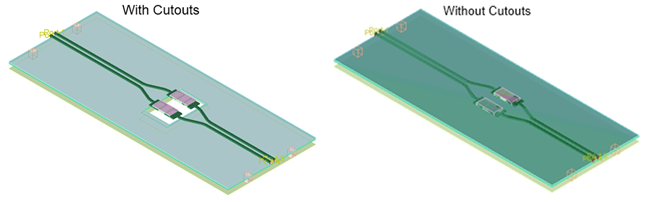
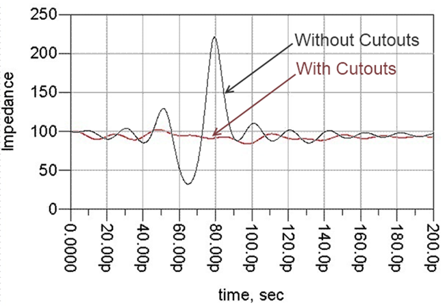
The following example compares the time-domain reflectometer (TDR) results of the DC blocking capacitor layout with and without the plane cutout improvements. With the plane cutouts properly applied using the above guidelines, the large discontinuity at the trace to DC blocking capacitor junction is eliminated.