Quartus® Prime Pro Edition User Guide: Design Constraints
ID
683143
Date
4/01/2024
Public
A newer version of this document is available. Customers should click here to go to the newest version.
1.1.2.1. Specify Instance-Specific Constraints in Assignment Editor
1.1.2.2. Specify NoC Constraints in NoC Assignment Editor
1.1.2.3. Specify I/O Constraints in Pin Planner
1.1.2.4. Plan Interface Constraints in Interface Planner and Tile Interface Planner
1.1.2.5. Adjust Constraints with the Chip Planner
1.1.2.6. Constraining Designs with the Design Partition Planner
3.2.1. Assigning to Exclusive Pin Groups
3.2.2. Assigning Slew Rate and Drive Strength
3.2.3. Assigning I/O Banks
3.2.4. Changing Pin Planner Highlight Colors
3.2.5. Showing I/O Lanes
3.2.6. Assigning Differential Pins
3.2.7. Entering Pin Assignments with Tcl Commands
3.2.8. Entering Pin Assignments in HDL Code
2.1.3.1. Placing NoC Design Elements Using Interface Planner
The following steps describe recommended placement of NoC design elements:
- Open, initialize, and load assignments in Interface Planner, as Interface Planner General Tool Flow describes.
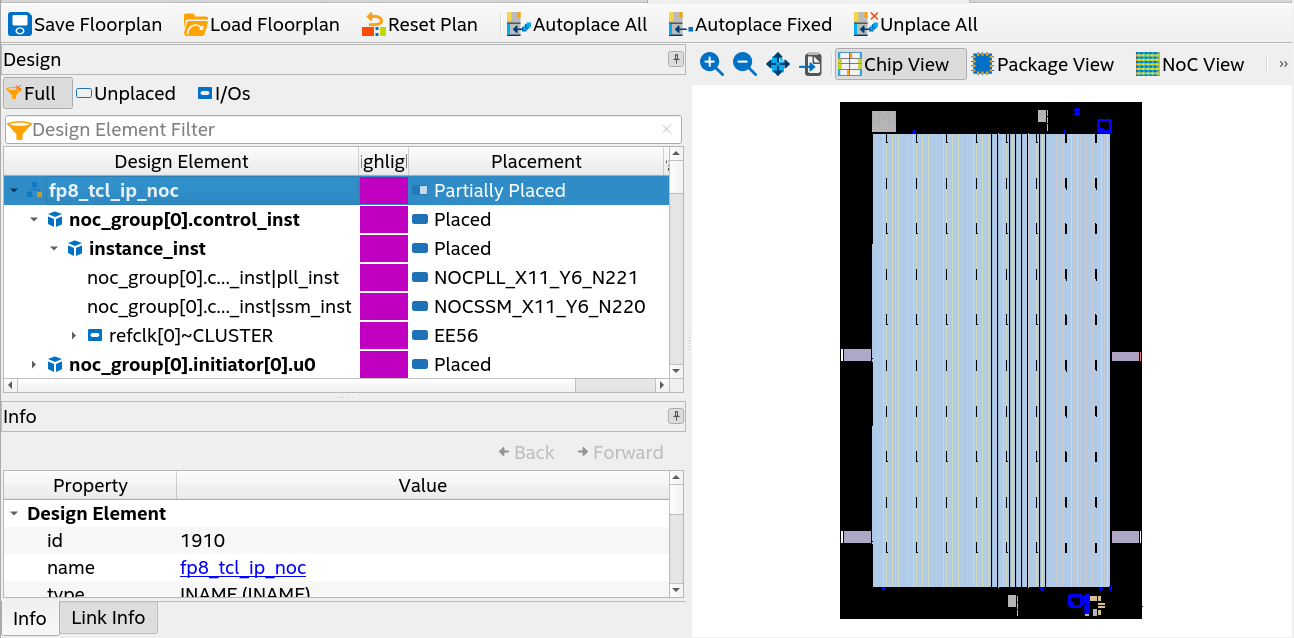
- Click Plan Design on the Flow control to interactively place NoC elements and other design elements in legal locations in the device periphery. All placeable elements, including NoC elements and periphery elements, appear in the Design Elements list. Refer to Recommended Placement Order for NoC Elements in Interface Planner.
- Use any of the following methods to place design elements in the Chip View:
- Drag NoC elements from the Design Elements list and drop them onto available device resources in the Chip view. You may experience a small delay while dragging as Interface Planner calculates the legal locations.
- To allow Interface Planner to place an unplaced design element in a legal location, right-click and select Autoplace Selected. You must use Autoplace Selected for all unplaced clocks.
- Right-click an element the Design Elements list, and then click Generate Legal Locations to display a list of Legal Locations for the element. Click any legal location in the list to highlight the location in the floorplan. Double-click any location in the list to place the element in the location.
- After making all necessary location assignments in Interface Planner, validate the placement by clicking Validate Plan in the Flow pane.
Figure 20. NoC Elements in Interface Planner Design Tab Chip View

- To generate a Tcl script to apply the placement constraints to your project, click Export Constraints in the Flow pane. To automatically run the Tcl script, enable Apply Assignments.
Figure 21. Export Physical Constraints from Interface Planner to Your Project
- To report whether the NoC initiator and target location placement allows your design to meet the bandwidth and transaction size requirements, click the Reports tab, and then double-click Report NoC Performance in the Tasks pane. For report details, refer to Report NoC Performance.