Developer Guide
FPGA Optimization Guide for Intel® oneAPI Toolkits
A newer version of this document is available. Customers should click here to go to the newest version.
FPGA Architecture Overview
A field-programmable gate array (FPGA) is a reconfigurable semiconductor integrated circuit (IC).
FPGAs occupy a unique computational niche relative to other computing devices, such as central and graphics processing units (CPUs and GPUs), and custom accelerators, such as application-specific integrated circuits (ASICs). CPUs and GPUs have a fixed hardware structure to which a program maps. Conversely, ASICs and FPGAs can build custom hardware to implement a program.
While a custom ASIC generally outperforms an FPGA on a specific task, they take significant time and money to develop. However, FPGAs are a cheaper off-the-shelf alternative that you can reprogram for each new application.
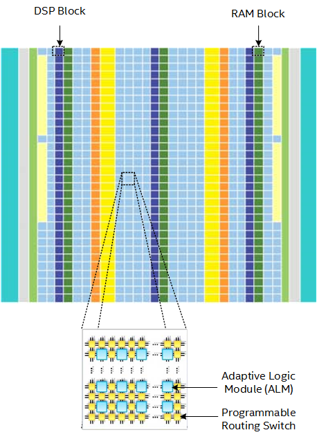
An FPGA is made up of a grid of configurable logic, known as adaptive logic modules (ALMs), and specialized blocks, such as digital signal processing (DSP) blocks and random-access memory (RAM) blocks. These programmable blocks are combined via configurable routing interconnects to implement complete digital circuits.
The total number of ALMs, DSP blocks, and RAM blocks used by a design is often referred to as the FPGA area or area that the design uses.
The following image illustrates a high-level architectural view of an FPGA: