AN 1014: Implementing Analog-to-Digital Converter Multilink Design with Agilex™ 7 FPGA F-Tile JESD204C RX IP
ID
857717
Date
11/24/2025
Public
1.1. ADC to Agilex™ 7 Dual Link Design Overview
1.2. ADC to Agilex™ 7 Dual Link Design Implementation Guidelines
1.3. Synchronized ADC to Agilex™ 7 Dual Link
1.4. Instantiating TX simplex into RX Multi-Link Design for Loopback Hardware Testing
1.5. Document Revision History for AN 1014: Implementing Analog-to-Digital Converter Dual Link Design with Agilex™ 7 FPGA F-Tile JESD204C RX IP
1.3.1.1. Editing Design Example Platform Designer System for Synchronized ADC to Agilex™ 7 Dual Link
1.3.1.2. Editing Design Example Top-Level HDL for Synchronized ADC to Agilex™ 7 Dual Link
1.3.1.3. Editing Simulation Testbench for Synchronized ADC to Agilex™ 7 Dual Link
1.3.1.4. Adding IP Signals to the Simulation Waveform
1.3.1.5. Updating the Simulation Script
1.3.1.6. Simulating the Dual Link Design
1.3.1.7. Viewing the Simulation Results
1.3.2.1. Editing Design Example Platform Designer System for Synchronized ADC to Agilex™ 7 Dual Link
1.3.2.2. Editing Design Example Top-Level HDL for Synchronized ADC to Agilex™ 7 Dual Link
1.3.2.3. Editing Design Example Top-Level SDC Constraint for Synchronized ADC to Agilex™ 7 Dual Link
1.3.2.4. Compiling the Design in Quartus® Prime Software
1.4. Instantiating TX simplex into RX Multi-Link Design for Loopback Hardware Testing
To test the dual RX design on hardware, you may instantiate its complementing JESD204C TX IP for each of the RX IP as follows:
- Open the Quartus® Prime project of the generated design example, jesd204c_f_ed_rx.qpf, in the ed/quartus/ folder.
- Open the top-level system, j204c_f_rx_ss.qsys, in Platform Designer. The RX .qsys file is located in the ed/rtl/rx/ folder.
- In the System View tab, right-click the j204c_f_rx_ip instance and select Drill into Subsystem. This opens the j204c_f_rx_ip Platform Designer subsystem.
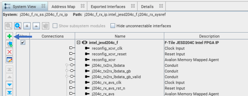
- Click the + button on the left side of the System View tab to add a new instance to the system.
Figure 20. Adding New Instance in Platform Designer
- Expand Interface Protocols and JESD. Select F-Tile JESD204C FPGA IP and click the Add button.
- In the Main tab and JESD204C Configurations tab, enter the same data rate as its interfacing RX IP. E.g if it is interfacing with an RX IP with a data rate of 16 Gbps, ensure the TX data rate is also set to 16 Gbps. Rename the IP as intel_jesd204c_f_tx_0 in the HDL entity name field.
- Since the two RX IPs in this design is identical, you may duplicate the TX IP created in step 6. Right-click the intel_jesd204c_f_tx_0 component and select Duplicate. This duplicates the F-Tile JESD204C FPGA IP. Rename the duplicated IP as intel_jesd204c_f_tx_1.
Note: Select No if the Platform Designer prompts the following: Do you want to also duplicate the IP Variant file on the disk? This is because the duplicated JESD204C FPGA IP has the same parameters as the original JESD204C FPGA IP.
- Connect j204c_pll_refclk and sysclk to out_refclk_fgt_6 and out_systempll_clk_0 of systemclk_f component respectively.
- Connect the duplicated IP port as shown in the following table:
Table 7. Connections for j204c_f_ip in Platform Designer for TX Simplexes Ports for Duplicated IP Connection j204c_pll_refclk systemclk_f.out_refclk_fgt_6 sysclk systemclk_f.out_systempll_clk_0 - Double click the export column to export all the F-Tile JESD204C FPGA IP ports except j204c_syspll_div2_clk.
- Move up one level of the hierarchy to j204c_f_ss; this is the top level of the Platform Designer system.
- Duplicate rxlink_clk and rxframe_clk component and rename to txlink_clk and txframe_clk respectively.
Note: Select Yes if the Platform Designer prompts the following: Do you want to also duplicate the IP Variant file on the disk?
- Connect txlink_clk.in_clk to ed_control.txlink_clk and export txlink_clk.out_clk.
- Export txframe_clk.in_clk.
- Connect the duplicated IP port as shown in the following table.
Table 8. Connections for j204c_f_ss in Platform Design for TX Simplexes Ports for Transmitter IP Connection reconfig_xcvr_clk mgmt_clk.out_clk reconfig_xcvr_reset reset_controller_0.reset_out reconfig_xcvr jtag_avmm_bridge.master j204c_txlink_clk ed_control.txlink_clk j204c_txframe_clk txframe_clk.out_clk j204c_tx_avs_clk mgmt_clk.out_clk j204c_tx_avs_rst_n rst_seq_0.reset_out1 j204_tx_avs mm_bridge.m0 - Change the connection of the j204c_rx_avs_rst_n port of the original F-Tile JESD204C RX IP to rst_seq_1.reset_out0. For j204c_tx_avs_rst_n port of the original F-Tile JESD204C TX IP, change its connection to rst_seq_0.reset_out1.
Note: You can assert the Avalon® memory-mapped interface reset for the IP control and status register (CSR) at the same time as the reconfig_xcvr_reset reset. Refer to the F-Tile JESD204C TX/RX Reset Sequence figure in the F-Tile JESD204C IP User Guide.
- Export the rest of the ports by clicking on the Double-click to export in the Export column of the System View tab.
- Disconnect j204c_tx2rx_lbdata, j204c_tx2rx_lbdata_gb, and j204c_tx2rx_lbdata_gb_valid at the original ports and export these ports. You may leave these ports as is if you intend to use them for debug purposes.
- At the address map, adjust the starting address of j204c_rx_avs and j204c_reconfig_xcvr interfaces so that there is no conflict with other components or interfaces. For example, you can set the starting address of the intel_jesd204c_f_1 IP to 0x000d_0400 as shown in the following table.
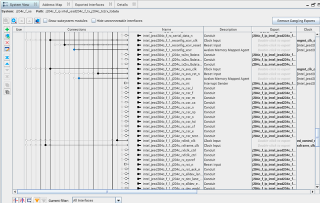
Table 9. Address Map for Design Example with TX Simplexes for Loopback Hardware Testing jtag_avmm_bridge.master mm_bridge.m0 j204c_f_rx_ip.intel_jesd204c_j204c_rx_avs N/A 0x000d_0000 – 0x000d_03ff j204c_f_rx_ip.intel_jesd204c_1_j204c_rx_avs N/A 0x000d_0400 – 0x000d_07ff j204c_f_ip.intel_jesd204c_f_tx_0_j204c_tx_avs N/A 0x000c_0000 – 0x000c_03ff j204c_f_ip.intel_jesd204c_f_tx_1_j204c_tx_avs N/A 0x000c_0400 – 0x000c_07ff j204c_f_rx_ip.intel_jesd204c_j204c_reconfig 0x0200_0000 – 0x021f_ffff 4 N/A j204c_f_rx_ip.intel_jesd204c_1_j204c_reconfig 0x0220_0000 – 0x023f_ffff 4 N/A j204c_f_ip.intel_jesd204c_f_tx_0_reconfig_xcvr 0x0240_0000 – 0x021f_ffff 4 N/A j204c_f_ip.intel_jesd204c_f_tx_1_reconfig_xcvr 0x0260_0000 – 0x023f_ffff 4 N/A - Repeat steps 4 through 12 for subsequent links in your design. Refer to the following figure for the screenshot of link 1 of the JESD204C IP.
Figure 21. Connections and Exports in Platform Designer
- Click Generate HDL to generate the design files needed for Quartus® Prime compilation.
- Ensure that you select the HDL language of your choice in the Simulation section of the Generation window to generate the simulation models.
- Click Generate and Yes to save and generate the design files needed for simulation.
- After the HDL generation is completed, select Generate from the menu of the Platform Designer. Select Show Instantiation Template…, and click Copy.
- Paste the instantiation template of j204c_f_ss Platform Designer into a text editor. You must update the instantiated Platform Designer ports at the top-level HDL.
- Click Finish to save your Platform Designer settings and exit the Platform Designer window.
- Add TX ports and wires into the top level:
// RX/TX serial data input/output
output wire [LINK*L-1:0]                     	tx_serial_data,
output wire [LINK*L-1:0]                     	tx_serial_data_n,
output wire [LINK-1:0]                            tx_link_error,

//Clock
wire                                       	  txlink_clk;
wire                                      	   txframe_clk;
wire                                       	  tx_fclk;

//Reset
wire [LINK-1:0]                            	  tx_rst;
wire [LINK-1:0]                            	  tx_rst_ack_n;
wire                                       	  mgmt_txlinkrst_n;

// j204c interface
wire [LINK-1:0]                            	  tx_avst_ready;
 wire [LINK-1:0]                            	 tx_avst_valid;
wire [LINK-1:0][(TOTAL_CS)-1:0]            	  tx_avst_control;

// CSR
wire [LINK-1:0][3:0]                     		tx_csr_l;
wire [LINK-1:0][7:0]                       	   tx_csr_f;
wire [LINK-1:0][7:0]                       	   tx_csr_m;
wire [LINK-1:0][1:0]                               tx_csr_cs;
wire [LINK-1:0][4:0]                       	   tx_csr_n;
wire [LINK-1:0][4:0]                       	   tx_csr_np;
wire [LINK-1:0][4:0]                      	    tx_csr_s;
wire [LINK-1:0]                            	   tx_csr_hd;
wire [LINK-1:0][4:0]                       	   tx_csr_cf;
wire [LINK-1:0][7:0]                       	   tx_csr_e;

//Sysref
wire [LINK-1:0]                            	   tx_sysref;

//Pattern
wire [LINK-1:0][L-1:0]                     	   tx_serial_data_reordered;
wire [LINK-1:0][L-1:0]                     	   tx_serial_data_n_reordered;
wire [LINK-1:0][(TOTAL_SAMPLE*N)-1:0]      	   tx_avst_data;

//cmd
wire [LINK-1:0][L*18-1:0]             		   tx_cmd_data;
wire [LINK-1:0][CMD_WIDTH-1:0]      		     j204c_tx_cmd_data;
wire [LINK-1:0]                       		   tx_cmd_valid;
wire [LINK-1:0]                       		   tx_cmd_ready;

wire [LINK-1:0]                         		 tx_link_error_mgmtclk;
- In the subsystem instance, update resets and clocks:
.rst_seq_0_reset_out3_reset                                 (tx_rst[0]),5

.txframe_clk_clk                                            (txframe_clk),
.txlink_clk_clk                                             (txlink_clk),
- Update the logics to include TX parameters:
assign user_led[3:0] = {~rx_patchk_data_error_reg[0], ~rx_link_error[0], ~tx_link_error[0], ~spi_prog_done}; assign ed_control_tst_err0_tst_error_i = {cmd_ramp_chk_err_mgmtclk[0], rx_link_error_mgmtclk[0], tx_link_error_mgmtclk[0], rx_patchk_data_error_mgmtclk[0]}; generate for (i=0; i<LINK; i=i+1) begin: GEN_SYSREF assign tx_sysref[i] = ed_ctrl_out_ip_sysref; assign rx_sysref[i] = ed_ctrl_out_ip_sysref; end endgenerate generate if (SH_CONFIG != 1) begin for(i=0; i<LINK; i=i+1) begin: LINK_map for (k=0;k<L;k=k+1) begin: cmd_data_map assign j204c_tx_cmd_data[i][k*6 +: 6] = tx_cmd_data[i][k*18 +: 6]; assign rx_cmd_data[i][k*18 +: 18] = {12'h0, j204c_rx_cmd_data[i][k*6 +: 6]} ; end end end else begin assign j204c_tx_cmd_data = tx_cmd_data; assign rx_cmd_data = j204c_rx_cmd_data ; end endgenerate - Add pattern and cmd generator block as well as other TX components:
generate
for (i=0; i<LINK; i=i+1) begin: GEN_BLOCK
	assign rx_serial_data_reordered[i] = rx_serial_data[i*L+L-1:i*L];
	assign rx_serial_data_n_reordered[i] = rx_serial_data_n[i*L+L-1:i*L];
	assign tx_serial_data[i*L+L-1:i*L] = tx_serial_data_reordered[i];
	assign tx_serial_data_n[i*L+L-1:i*L] = tx_serial_data_n_reordered[i];
	j204c_f_pat_gen_top #(
		.WIDTH_MULP        (WIDTH_MULP),
		.M                 (M),
		.N                 (N),
		.S                 (S),
		.CS                (CS),
		.TOTAL_CS          (TOTAL_CS),
		.REVERSE_DATA      (0)
		) u_gen (
		.clk               (txframe_clk),
		.rst_n             (~tx_rst[0]),
		.sync_clr_n        (1'b1),//wailoonn
		.ready             (tx_avst_ready[i]),
		.patgen_en         (1'b1),
		.prbs_test_ctl     (prbs_test_ctl),
		.ramp_test_ctl     (ramp_test_ctl),
		.error_inject      (1'b0),
		.valid             (tx_avst_valid[i]),
		.avst_ctlout       (tx_avst_control[i]),
		.avst_dataout      (tx_avst_data[i])
	);

j204c_f_cmd_gen_top #(
		.L              (L),
		.SL_CMD         (SL_CMD),
		.ED_CMD_RMP_EN  (ED_CMD_RMP_EN),
		.SH_CONFIG      (SH_CONFIG)
		) cmd_gen_inst (
		.link_clk       (txlink_clk),
		.rst_n          (~tx_rst[0]),
		.i_ready        (tx_cmd_ready[i]),
		.o_cmd_valid    (tx_cmd_valid[i]),
		.o_cmd_data     (tx_cmd_data[i])
	);

assign tx_link_error_mgmtclk = tx_link_error;
- Assign pins in the QSF accordingly and compile.
- Open main.tcl script in the hwtest folder. Modify the script to include the added links.
- Set the clock controller to reflect refclk frequency defined in IP GUI.
- Program sof into board.
- Open the system console and modify the master path to point to the correct device.
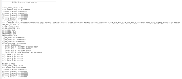
- Run start_basic_test command.
The following figure shows the expected result in system console:Figure 22. Example Result in System Console
4 The address span of the PHY reconfiguration interface depends on the number of transceiver channels.
5 Existing instance, update by adding tx_rst[0] into the parethesis.