AN 1014: Implementing Analog-to-Digital Converter Multilink Design with Agilex™ 7 FPGA F-Tile JESD204C RX IP
ID
857717
Date
11/24/2025
Public
1.1. ADC to Agilex™ 7 Dual Link Design Overview
1.2. ADC to Agilex™ 7 Dual Link Design Implementation Guidelines
1.3. Synchronized ADC to Agilex™ 7 Dual Link
1.4. Instantiating TX simplex into RX Multi-Link Design for Loopback Hardware Testing
1.5. Document Revision History for AN 1014: Implementing Analog-to-Digital Converter Dual Link Design with Agilex™ 7 FPGA F-Tile JESD204C RX IP
1.3.1.1. Editing Design Example Platform Designer System for Synchronized ADC to Agilex™ 7 Dual Link
1.3.1.2. Editing Design Example Top-Level HDL for Synchronized ADC to Agilex™ 7 Dual Link
1.3.1.3. Editing Simulation Testbench for Synchronized ADC to Agilex™ 7 Dual Link
1.3.1.4. Adding IP Signals to the Simulation Waveform
1.3.1.5. Updating the Simulation Script
1.3.1.6. Simulating the Dual Link Design
1.3.1.7. Viewing the Simulation Results
1.3.2.1. Editing Design Example Platform Designer System for Synchronized ADC to Agilex™ 7 Dual Link
1.3.2.2. Editing Design Example Top-Level HDL for Synchronized ADC to Agilex™ 7 Dual Link
1.3.2.3. Editing Design Example Top-Level SDC Constraint for Synchronized ADC to Agilex™ 7 Dual Link
1.3.2.4. Compiling the Design in Quartus® Prime Software
1.3.1.2. Editing Design Example Top-Level HDL for Synchronized ADC to Agilex™ 7 Dual Link
The generate statement in the Verilog HDL file uses the LINK system parameter as an index variable to generate the requisite number of instances for the dual link use case.
- Open the top-level HDL file (jesd204c_f_ed.sv) in the simulation/models/ folder in a text editor.
- Modify the LINK system parameter to reflect the number of links in your design.
- Insert the newly exported ports from the j204c_f_ss Platform Designer system instantiation.
- To make the connections for the Platform Designer ports:
- For RX link reset and frame reset, distribute the rx_rst[0] wire from the reset sequencer in Platform Designer to the IPs and pattern checkers of the second and subsequent links. One way to achieve this is to hard code the index in the rx_rst[i] wire in the pattern checker and the synchronizer (j204c_pulse_CDC) instantiations generation loop with rx_rst[0]. Refer to the following figures for the RX reset distribution.
Figure 7. JESD204C RX IP Link Reset
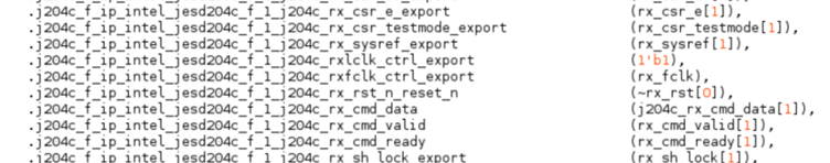 Figure 8. Pattern Checker for the Frame Reset for the Data Channel and Link Reset for the Command Channel
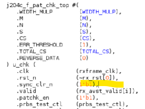
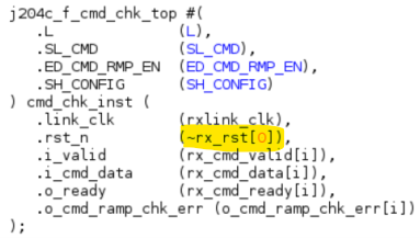 Figure 9. JESD204C RX IP, Data Channel, and Command Channel Pattern Checker Error Flag Synchronizer Reset
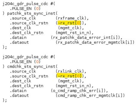 Figure 10. Sysref Synchronizer Reset
- b. For TX link reset and frame reset, distribute the tx_rst[0] wire from the reset sequencer in Platform Designer to the IPs and pattern generators of the second and subsequent links. One way to achieve this is to hard code the index in the tx_rst[i] wire in the pattern generator instantiation generation loop with tx_rst[0].
Figure 11. JESD204C TX IP Link Reset and Pattern Generator
- Change the dimension of the following wires. This example is shown in Verilog HDL:
- wire [LINK-1:0] j204c_rx_dev_lane_align;
- wire [LINK-1:0] j204c_rx_dev_emblock_align;
- Add an index to the following wires at the Platform Designer ports of the JESD204C RX IP. Use index [0] for link 0, index [1] for link 1, and so forth. Example:
- j204c_rx_dev_lane_align[0]
- j204c_rx_dev_emblock_align[0]
- Connect the j204c_rx_dev_lane_align port of each IP to an AND gate. Distribute the output of the AND gate to the j204c_rx_alldev_lane_align port of each IP.
// Example in Verilog
assign j204c_rx_alldev_lane_align = &j204c_rx_dev_lane_align;
- Connect the j204c_rx_dev_emblock_align port of each IP to an AND gate. Distribute the output of the AND gate to the j204c_rx_alldev_emblock_align port of each IP.
// Example in Verilog
assign j204c_rx_alldev_emblock_align = &j204c_rx_dev_emblock_align;
- For the rest of the ports, increase the index wires from 0 to 1, and use subsequent numbers for the subsequent links.
Example: The rx_avst_data[1] wire should be connected to link 1 IP.
- h. Ensure to assign multilink signals accordingly at the ports.
// Example in Verilog
.j204c_f_ip_intel_jesd204c_f_1_j204c_rx_alldev_lane_align_export (j204c_rx_alldev_lane_align),
.j204c_f_ip_intel_jesd204c_f_1_j204c_rx_dev_lane_align_export (j204c_rx_dev_lane_align[1]),
.j204c_f_ip_intel_jesd204c_f_1_j204c_rx_alldev_emblock_align_export(j204c_rx_alldev_emblock_align),
.j204c_f_ip_intel_jesd204c_f_1_j204c_rx_dev_emblock_align_export (j204c_rx_dev_emblock_align[1]),
- For RX link reset and frame reset, distribute the rx_rst[0] wire from the reset sequencer in Platform Designer to the IPs and pattern checkers of the second and subsequent links. One way to achieve this is to hard code the index in the rx_rst[i] wire in the pattern checker and the synchronizer (j204c_pulse_CDC) instantiations generation loop with rx_rst[0]. Refer to the following figures for the RX reset distribution.
- Connect the j204c_rx_emb_lock output port of each IP to the input of an AND gate. Connect the output of the AND gate to the emb_lock_out output port of the design example. Perform a similar action for the rx_sh_lock port.
// Example in Verilog
assign emb_lock_out = &rx_emb_lock;
assign sh_lock_out = &rx_sh_lock;
- For subclass 1 subsystem, comment out or delete the sysref_out port and its assignment. SYSREF should be sourced from the clock generator, which supplies the device clock to the ADC and the FPGA. The fpga_sysref signal from ED Control block is meant for debug purpose only.
// Example in Verilog // output wire sysref_out, // assign sysref_out = fpga_sysref; - Disable rst_seq_1_reset_out0_reset port as this port is now being used for j204c_rx_avs_rst_n signal.
// Example in Verilog // .rst_seq_1_reset_out0_reset (rx_unused0_rst_n), - Save the top-level HDL file changes.