AN 1014: Implementing Analog-to-Digital Converter Multilink Design with Agilex™ 7 FPGA F-Tile JESD204C RX IP
ID
857717
Date
11/24/2025
Public
1.1. ADC to Agilex™ 7 Dual Link Design Overview
1.2. ADC to Agilex™ 7 Dual Link Design Implementation Guidelines
1.3. Synchronized ADC to Agilex™ 7 Dual Link
1.4. Instantiating TX simplex into RX Multi-Link Design for Loopback Hardware Testing
1.5. Document Revision History for AN 1014: Implementing Analog-to-Digital Converter Dual Link Design with Agilex™ 7 FPGA F-Tile JESD204C RX IP
1.3.1.1. Editing Design Example Platform Designer System for Synchronized ADC to Agilex™ 7 Dual Link
1.3.1.2. Editing Design Example Top-Level HDL for Synchronized ADC to Agilex™ 7 Dual Link
1.3.1.3. Editing Simulation Testbench for Synchronized ADC to Agilex™ 7 Dual Link
1.3.1.4. Adding IP Signals to the Simulation Waveform
1.3.1.5. Updating the Simulation Script
1.3.1.6. Simulating the Dual Link Design
1.3.1.7. Viewing the Simulation Results
1.3.2.1. Editing Design Example Platform Designer System for Synchronized ADC to Agilex™ 7 Dual Link
1.3.2.2. Editing Design Example Top-Level HDL for Synchronized ADC to Agilex™ 7 Dual Link
1.3.2.3. Editing Design Example Top-Level SDC Constraint for Synchronized ADC to Agilex™ 7 Dual Link
1.3.2.4. Compiling the Design in Quartus® Prime Software
1.3.1.1. Editing Design Example Platform Designer System for Synchronized ADC to Agilex™ 7 Dual Link
- Generate an example design with data path set to receiver with Multilink Mode enabled.
- Open the Quartus® Prime project of the generated design example, jesd204c_f_ed.qpf, in the simulation/models/ folder.
- Open the top-level system, j204c_f_ss.qsys, in Platform Designer. The RX .qsys file is located in the simulation/models/ folder.
- In the System View tab, right-click the j204c_f_ip instance and select Drill into Subsystem. This opens the j204c_f_ip Platform Designer subsystem.
- Right-click the intel_jesd204c_f component and select Duplicate.
This duplicates the RX Simplex F-Tile JESD204C FPGA IP. Rename the duplicated IP as intel_jesd204c_f_1.Note: Select No if the Platform Designer prompts the following: Do you want to also duplicate the IP Variant file on the disk? This is because the duplicated F-Tile JESD204C IP has the same parameters as the original F-Tile JESD204C IP .
- Repeat 4 for intel_jesd204c_f_tx component to duplicate TX Simplex F-Tile JESD204C IP. Rename the duplicated IP as intel_jesd204c_f_tx_1.
- Connect the duplicated IP port as shown in the following table.
Table 2. Connections for j204c_f_ip in Platform Designer for Simulation Ports for Duplicated IP Connection j204c_pll_refclk systemclk_f.out_refclk_fgt_6 sysclk systemclk_f.out_systempll_clk_0 - Double click at the export column to export all the F-Tile JESD204C IP ports except for the j204c_syspll_div2_clk port.
- Move up one level of the hierarchy to j204c_rx_ss; this is the top level of the Platform Designer system.
- Connect the duplicated IP port as shown in the following table.
Table 3. Connections for j204c_f_ss in Platform Designer for Simulation Ports for Duplicated IP Connection reconfig_xcvr_clk mgmt_clk.out_clk reconfig_xcvr_reset reset_controller_0.reset_out reconfig_xcvr jtag_avmm_bridge.master j204c_rx_avs_clk mgmt_clk.out_clk j204c_rx_avs_rst_n rst_seq_1.reset_out0 1 j204c_rx_avs mm_bridge.m0 j204c_rxlink_clk ed_control.rxlink_clk j204c_rxframe_clk rxframe_clk.out_clk j204c_txlink_clk ed_control.txlink_clk j204c_txframe_clk txframe_clk.out_clk j204c_tx_avs_clk mgmt_clk.out_clk j204c_tx_avs_rst_n rst_seq_0.reset_out1 j204c_tx_avs mm_bridge.m0 - Change the connection of the j204c_rx_avs_rst_n port of the original F-Tile JESD204C IP to rst_seq_1.reset_out0. For j204c_tx_avs_rst_n port of the original F-Tile JESD204C TX IP, change its connection to rst_seq_0.reset_out1.
Note: You can assert the Avalon® memory-mapped interface reset for the IP control and status register (CSR) at the same time as the reconfig_xcvr_reset reset. Refer to the F-Tile JESD204C TX/RX Reset Sequence figure in the F-Tile JESD204C IP User Guide.
- Export the rest of the ports by clicking on the Double-click to export in the Export column of the System View tab.
- Disconnect j204c_tx2rx_lbdata, j204c_tx2rx_lbdata_gb and j204c_tx2rx_lbdata_gb_valid at the original ports and export these ports. You may leave these ports as it is if you wished to use them for debug purposes.
- At the address map, adjust the starting address of j204c_rx_avs and j204c_reconfig_xcvr interfaces so that there is no conflict with other components or interfaces. For example, you can set the starting address of the intel_jesd204c_f__1 IP to 0x000d_0400 as shown in the following table.
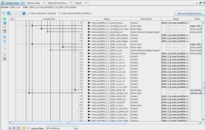
Table 4. Synchronized ADC-FPGA Dual Link Address Map for Design Example with System Console Control jtag_avmm_bridge.master mm_bridge.m0 j204c_f_ip.intel_jesd204c_f_j204c_rx_avs N/A 0x000d_0000 – 0x000d_03ff j204c_f_ip.intel_jesd204c_f_1_j204c_rx _avs N/A 0x000d_0400 – 0x000d_07ff j204c_f_ip.intel_jesd204c_f_tx_j204c_tx_avs N/A 0x000c_0000 – 0x000c_03ff j204c_f_ip.intel_jesd204c_f_tx_1_j204c_tx _avs N/A 0x000c_0400 – 0x000c_07ff j204c_f_ip.intel_jesd204c_j204c_reconfig_xcvr 0x0200_0000 – 0x021f_ffff 2 N/A j204c_f_ip.intel_jesd204c_1_j204c_reconfig_xcvr 0x0220_0000 – 0x023f_ffff 2 N/A - Repeat step 5 through step 12 for subsequent links in your design. Refer to the following figure for the screenshot of link 1 of the JESD204C IP.
- Click Generate HDL to generate the design files needed for Quartus® Prime compilation.
- Ensure that you select the HDL language of your choice in the Simulation section of the Generation window to generate the simulation models.
- Click Generate and Yes to save and generate the design files needed for simulation.
- After the HDL generation is completed, select Generate from the menu of the Platform Designer. Select Show Instantiation Template…, and click Copy.
- Paste the instantiation template of j204c_rx_ss Platform Designer into a text editor.
You must update the instantiated Platform Designer ports at the top-level HDL.
- Click Finish to save your Platform Designer settings, and exit the Platform Designer window.
Related Information
1 This port is originally exported. Double-click the reset_out0 port under rst_seq_1 component to disable the export so connection can be made.
2 The address span of the PHY reconfiguration interface depends on the number of transceiver channels.