External Memory Interfaces (EMIF) IP User Guide: Agilex™ 3 FPGAs and SoCs
A newer version of this document is available. Customers should click here to go to the newest version.
3.5.3. Advanced: Analog Overrides Tab
This tab contains two groups of parameters: Overrides and Values. The tables which follow provide descriptions of the parameters on this tab.
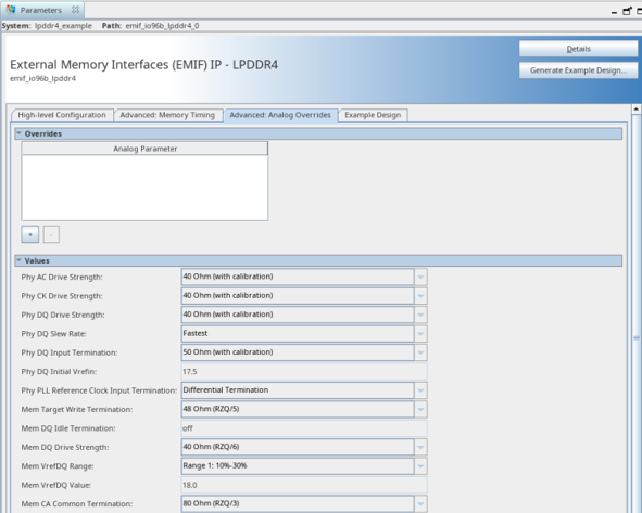
| Parameter Name | Description |
|---|---|
| Analog Parameter | Name of Analog Parameter to explicitly override; the values will be applied and appear in the list below. Default value is Legal values are: PHY_TERM_X_R_S_AC_OUTPUT_OHM, PHY_TERM_X_R_S_CK_OUTPUT_OHM, PHY_TERM_X_R_S_DQ_OUTPUT_OHM, PHY_TERM_X_DQ_SLEW_RATE, PHY_TERM_X_R_T_DQ_INPUT_OHM, PHY_TERM_X_DQ_VREF, PHY_TERM_X_R_T_REFCLK_INPUT_OHM, MEM_ODT_DQ_X_TGT_WR, MEM_ODT_DQ_X_IDLE, MEM_ODT_DQ_X_RON, MEM_VREF_DQ_X_RANGE, MEM_VREF_DQ_X_VALUE, MEM_ODT_CA_X_CA_COMM, MEM_ODT_CA_X_CA_ENABLE, MEM_ODT_CA_X_CS_ENABLE, MEM_ODT_CA_X_CK_ENABLE, MEM_VREF_CA_X_CA_RANGE, MEM_VREF_CA_X_CA_VALUE (Identifier: ANALOG_PARAM_DERIVATION_PARAM_NAME) |
| Parameter Name | Description |
|---|---|
| AC Drive Strength | This parameter allows you to change the input on chip termination settings for the selected I/O standard on the refclk input pins. Perform board simulation with IBIS models to determine the best settings for your design. Legal values are: SERIES_34_OHM_CAL, SERIES_40_OHM_CAL (Identifier: PHY_TERM_X_R_S_AC_OUTPUT_OHM) |
| CK Drive Strength | This parameter allows you to change the output on chip termination settings for the selected I/O standard on the CK Pins. Perform board simulation with IBIS models to determine the best settings for your design. Legal values are: SERIES_34_OHM_CAL, SERIES_40_OHM_CAL (Identifier: PHY_TERM_X_R_S_CK_OUTPUT_OHM) |
| FPGA DQ Drive Strength | This parameter allows you to change the output on chip termination settings for the selected I/O standard on the DQ Pins. Perform board simulation with IBIS models to determine the best settings for your design. Legal values are: SERIES_34_OHM_CAL, SERIES_40_OHM_CAL (Identifier: PHY_TERM_X_R_S_DQ_OUTPUT_OHM) |
| DQ Slew Rate | Specifies the slew rate of the data bus pins. The slew rate (or edge rate) describes how quickly the signal can transition, measured in voltage per unit time. Perform board simulations to determine the slew rate that provides the best eye opening for the data bus signals. Legal values are: SLOW, MEDIUM, FAST, FASTEST (Identifier: PHY_TERM_X_DQ_SLEW_RATE) |
| DQ Input Termination | This parameter allows you to change the input on chip termination settings for the selected I/O standard on the DQ Pins. Perform board simulation with IBIS models to determine the best settings for your design. Legal values are: RT_40_OHM_CAL, RT_50_OHM_CAL, RT_60_OHM_CAL (Identifier: PHY_TERM_X_R_T_DQ_INPUT_OHM) |
| DQ Initial Vrefin | Specifies the initial value for the reference voltage on the data pins(Vrefin). The specified value serves as a starting point and may be overridden by calibration to provide better timing margins. Legal values are: from 0 to 100 (Identifier: PHY_TERM_X_DQ_VREF) |
| PLL Reference Clock Input Termination | This parameter allows you to change the input on chip termination settings for the selected I/O standard on the refclk input pins. Perform board simulation with IBIS models to determine the best settings for your design. Legal values are: RT_OFF, RT_DIFF (Identifier: PHY_TERM_X_R_T_REFCLK_INPUT_OHM) |
| Target Write Termination | Specifies the target termination to be used during a write. The value of this parameter represents X, where: termination = RZQ/X = (240 Ohm)/X. Legal values are: off, 1, 2, 3, 4, 5, 6 (Identifier: MEM_ODT_DQ_X_TGT_WR) |
| DQ Idle Termination | Specifies the termination to be used for RTT_PARK and DQS_RTT_PARK. For power savings it is recommended to leave this as disabled. The value of this parameter represents X, where: termination = RZQ/X = (240 Ohm)/X. (Identifier: MEM_ODT_DQ_X_IDLE) |
| Memory DQ Drive Strength | Specifies the termination to be used when driving read data from memory. The value of this parameter represents X, where: termination = RZQ/X = (240 Ohm)/X. Legal values are: 6, 5, 4, 3, 2, 1 (Identifier: MEM_ODT_DQ_X_RON) |
| VrefDQ Range | Specifies which of the memory protocol defined ranges will be used. Legal values are: 1, 2 (Identifier: MEM_VREF_DQ_X_RANGE) |
| VrefDQ Value | Specifies the initial VrefDQ value to be used. Legal values are: from 15.00 to 44.90, from 10.00 to 30.00, from 32.90 to 62.90, from 22.00 to 42.00 (Identifier: MEM_VREF_DQ_X_VALUE) |
| CA Common Termination | Common termination value that can be applied to CA/CK/CS. The value of this parameter represents X, where: termination = RZQ/X = (240 Ohm)/X. "off" means this termination is disabled. Legal values are: off, 1, 2, 3, 4, 5, 6 (Identifier: MEM_ODT_CA_X_CA_COMM) |
| CA Termination Enable | Enable the common termination value on the CA bus. Enabling CA termination will have no effect unless the ODT_CA bond pad is HIGH.. The value of this parameter represents X, where: termination = RZQ/X = (240 Ohm)/X. "off" means this termination is disabled. Legal values are: false, true (Identifier: MEM_ODT_CA_X_CA_ENABLE) |
| CS Termination Enable | Enable the common termination value on the CS bus. The value of this parameter represents X, where: termination = RZQ/X = (240 Ohm)/X. "off" means this termination is disabled. Legal values are: false, true (Identifier: MEM_ODT_CA_X_CS_ENABLE) |
| CK Termination Enable | Enable the common termination value on the CK bus. The value of this parameter represents X, where: termination = RZQ/X = (240 Ohm)/X. "off" means this termination is disabled. Legal values are: false, true (Identifier: MEM_ODT_CA_X_CK_ENABLE) |
| VrefCA Range | Specifies which of the memory protocol defined ranges will be used. Legal values are: 1, 2 (Identifier: MEM_VREF_CA_X_CA_RANGE) |
| VrefCA Value | Specifies the initial VrefCA value to be used. Legal values are: from 10.00 to 30.00, from 22.00 to 42.00 (Identifier: MEM_VREF_CA_X_CA_VALUE) |