2.6. Compiling and Testing the Design Example
The JESD204B Intel® FPGA IP parameter editor allows you to run the design example on a target development kit.
Perform the following steps to compile the design and program the development board:
- Launch the Quartus® Prime software.
- In the Quartus® Prime software, open the Quartus® Prime project <example_design_directory>/ed_synth/intel_jesd204b_gts_ed_<data path>.qpf.
- Compile the design (Processing > Start Compilation).
The timing constraints and pin assignments for the design example and the design components are automatically loaded during design example compilation.
- Connect the development board to the host computer either by connecting a USB cable to the on-board Intel® FPGA Download Cable II component or using an external Intel® FPGA Download Cable II module to connect to the external JTAG connector.
- Launch the Clock Control application that is included with the development board, and set the clock settings according to the selected data rate.
Once downloaded, unzip the Installer Package to your PC. Navigate to the following path: agilex5e-prem-es-a5ed065bb32ae6sr0-v24-3-1b89-v1-0\examples\board_test_systemNote: Build number and version may vary.
- To launch the Clock Controller GUI, launch the Board Test System application using one of the following scripts depending on your host OS:
- Windows: start.bat
- Linux: start.sh
Note:On Windows systems, the start.bat script might be blocked and unable to run as it is an unrecognized app. You may need to adjust the properties of the .bat script to allow it to run. Right click on start.bat and click on Properties. Under the General tab, in the Security section, check the Unblock checkbox. Then click on OK. Rerun the start.bat.
On Linux systems, make the start.sh script executable by running the following command in terminal: $ chmod 777 start.sh
- After the Board Test System application is launched, click on Clock to load the Clock Controller GUI.
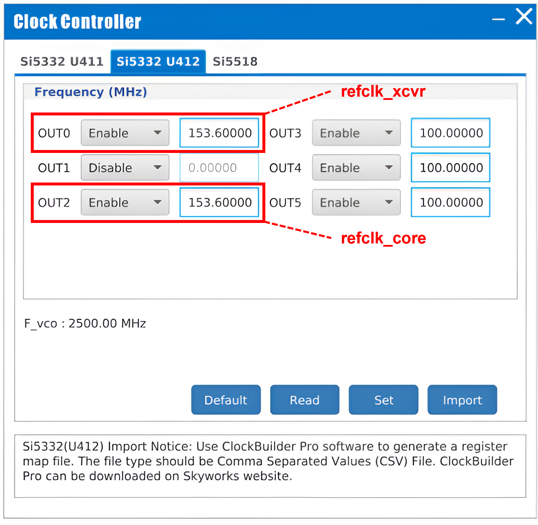
Table 7. Clock Settings Clock Name Clock Frequency refclk_xcvr Select the frequency for the transceiver PLL reference clock in the IP parameter editor. refclk_core Select the frequency for the core PLL reference clock in the IP parameter editor. mgmt_clk 100 MHz Figure 7. Clock Control GUI SettingThis example shows the clock control GUI setting for a design example on a GTS device using the Agilex™ 5 E-Series Premium Development Kit.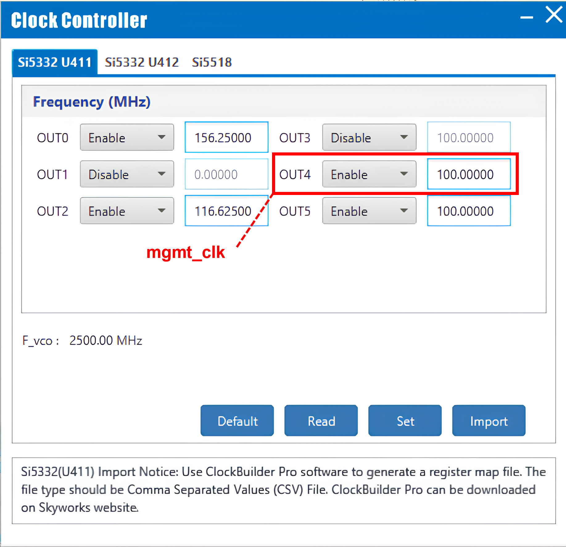
 Note: For dual simplex example designs that require a reference clock frequency other than the default 153.6 MHz, the Si5518 clock chip needs to be programmed via a clock profile using the ClockBuilder Pro software.
 - If you are performing external loopback test, attach the QSFP+ loopback module at cage QSFP2 (J13) for L=4 configuration. For L>4 configuration, attach another QSFP+ module at QSFP1 (J12).
- Configure the FPGA on the development board with the generated programming file (.sof file) using the Quartus® Prime Programmer.
To run the hardware testing using the Tcl script, refer to the Hardware Test for System Console Control Design Example section.