2.4. Dual Simplex Design Example
Figure 4. Dual Simplex Design Example Block Diagram
The Dual Simplex example design currently supports Duplex Case only with TX and RX in the same or mixed configuration, e.g. data rate, number of lanes (L), number of converters per device (M), number of octets per frame (F), etc. For more information, refer to the Dual Simplex Support section in the GTS JESD204B Intel® FPGA IP User Guide.
To generate the design example:
- Create a project targeting Agilex™ 5 or Agilex™ 3 device family and select the desired device.
- In the IP Catalog, Tools > IP Catalog, select GTS JESD204B Intel® FPGA IP . Modify the IP Tab for required JESD configurations. The JESD IP supports same or mixed configuration for both TX and RX. Set the data path as Duplex mode.
- In the GTS JESD204B Intel® FPGA IP GUI, go to the Example Design tab and enable Enable dual simplex generation.
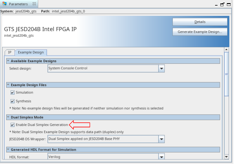
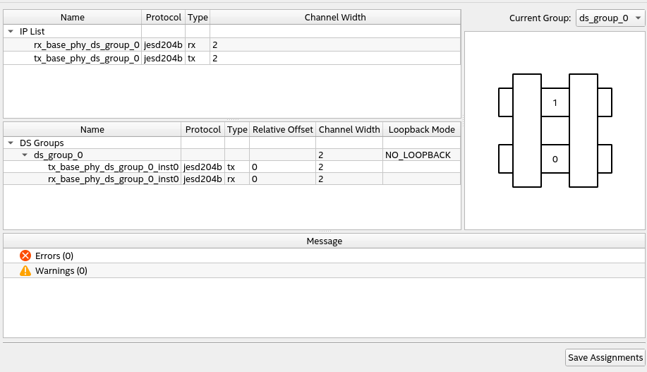
- Generate the example design and after opening the example design, choose the Dual Simplex assignment editor in the Assignments menu.
- Verify the TX and RX PHY relative offsets. Save assignments and run IP generation in Quartus® Prime. This will generate the HSSI dual simplex generation.
- Run the full compilation and perform the hardware test according to Hardware Test for System Console Control Design Example.