High Bandwidth Memory (HBM2E) Interface Intel Agilex® 7 M-Series FPGA IP User Guide
ID
773264
Date
4/21/2023
Public
A newer version of this document is available. Customers should click here to go to the newest version.
1. About the High Bandwidth Memory (HBM2E) Interface Intel Agilex® 7 FPGA IP User Guide
2. Introduction to High Bandwidth Memory
3. Intel Agilex® 7 M-Series HBM2E Architecture
4. Creating and Parameterizing the High Bandwidth Memory (HBM2E) Interface Intel® FPGA IP
5. High Bandwidth Memory (HBM2E) Interface Intel® FPGA IP Interface
6. High Bandwidth Memory (HBM2E) Interface Intel® FPGA IP Controller Performance
7. Document Revision History for High Bandwidth Memory (HBM2E) Interface Intel FPGA IP User Guide
A. High Bandwidth Memory (HBM2E) Interface Intel® FPGA IP Intel® Quartus® Prime Software Flow
3.5. Intel Agilex® 7 M-Series HBM2E Controller Architecture
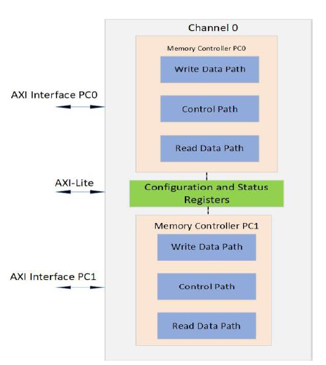
The hardened HBM2E controller provides a total of sixteen controller cores, one per Pseudo Channel.
Each controller consists of a write and read data path and the control logic that helps to translate user commands to the HBM2E memory. The HBM2E controller logic accounts for the HBM2E memory specification timing and schedules commands in an efficient manner. The following figure shows a block diagram of the HBM2E controller, corresponding to channel 0. You can find more information about the interface timing details in the User AXI Interface Timing section.
Figure 6. Intel Agilex® 7 M-Series HBM2E Controller Block Diagram