AN 692: Power Sequencing Considerations for Cyclone® 10 GX, Arria® 10, Stratix® 10, Agilex™ 7, and Agilex™ 5 Devices
1.1.2.2. Low-Cost Discrete Sequencer Simulation Results
Figure 5. Circuit Simulation Results for Power-Up and Power-Down Events
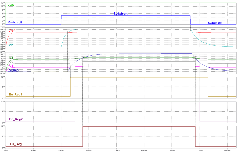
Power ON
Initially, the power sequencer circuit is not operational because the power switch S1 is open. As a result, all regulator enables (En_Reg1, En_Reg2, and En_Reg3) are low. As the regulator enables drive the voltage regulators, all voltage regulators are turned off.- When switch S1 is closed, the system turns on and the voltage VCC charges the capacitor C1 to voltage level Vin.
- C1 is charged through resistor R1. Voltage level Vin depends on the values of R1 and R2 which form voltage divider and Vin = (R2/(R1+R2))*VCC. R1 and R2 are selected such that the value of Vin is slightly higher than comparator U1A's reference voltage Vref.
- When the value of Vin rises above Vref, comparator U1A's output goes high and capacitor C4 starts charging through resistor R5.
- Resistors R5 and R6 set the ramp voltage Vramp. Resistor R5 and capacitor C4 define the time constant for the ramp rate of Vramp. Vramp is the input voltage to the non-inverting inputs of comparators U1B, U1C, and U1D. As Vramp rises above the voltage references (V1, V2, and V3), it sequentially trips comparators U1D, U1C, and U1B, turning on regulator enables En_Reg1, En_Reg2, and En_Reg3.
Power OFF
- The order of the power-down sequence is reverse of the power-up sequence.
- When switch S1 is opened, the system starts shutting down. Capacitor C1 starts discharging through R2. R2 and C1 set the decay rate of Vin during the power-down cycle.
- When Vin falls below Vref, comparator U1A's output turns off. This discharges Vramp through the parallel combination of R5 and R6.
- As Vramp discharges below V3, V2, and V1, the comparators U1B, U1C and U1D sequentially turn off their regulator enables.
This example circuit can be easily expanded to support more regulator enable (reg_en) outputs.
To expand the circuit, add more comparators and extend the resistor ladder network to generate additional reference voltage comparison points (for example, V4, V5, etc). Also, increase the Vramp charging/discharging rate to allow more time between the additional regulator enables. This time delay is controlled by the time constant determined by R5, R6, and C4.