A newer version of this document is available. Customers should click here to go to the newest version.
1. Intel® Stratix® 10 Embedded Memory Overview
2. Intel® Stratix® 10 Embedded Memory Architecture and Features
3. Intel® Stratix® 10 Embedded Memory Design Considerations
4. Intel® Stratix® 10 Embedded Memory IP References
5. Intel Stratix 10 Embedded Memory Design Example
6. Intel® Stratix® 10 Embedded Memory User Guide Archives
7. Document Revision History for the Intel® Stratix® 10 Embedded Memory User Guide
2.1. Byte Enable in Intel® Stratix® 10 Embedded Memory Blocks
2.2. Address Clock Enable Support
2.3. Asynchronous Clear and Synchronous Clear
2.4. Memory Blocks Error Correction Code Support
2.5. Force-to-Zero
2.6. Coherent Read Memory
2.7. Freeze Logic
2.8. True Dual Port Dual Clock Emulator
2.9. 'X' Propagation Support in Simulation
2.10. Intel® Stratix® 10 Supported Embedded Memory IPs
2.11. Intel® Stratix® 10 Embedded Memory Clocking Modes
2.12. Intel® Stratix® 10 Embedded Memory Configurations
2.13. Initial Value of Read and Write Address Registers
3.1. Consider the Memory Block Selection
3.2. Consider the Concurrent Read Behavior
3.3. Customize Read-During-Write Behavior
3.4. Consider Power-Up State and Memory Initialization
3.5. Reduce Power Consumption
3.6. Avoid Providing Non-Deterministic Input
3.7. Avoid Changing Clock Signals and Other Control Signals Simultaneously
3.8. Including the Reset Release Intel® FPGA IP in Your Design
4.1.1. Release Information for RAM and ROM Intel® FPGA IPs
4.1.2. RAM: 1-PORT Intel® FPGA IP Parameters
4.1.3. RAM: 2-PORT Intel® FPGA IP Parameters
4.1.4. RAM: 4-PORT Intel® FPGA IP Parameters
4.1.5. ROM: 1-PORT Intel® FPGA IP Parameters
4.1.6. ROM: 2-PORT Intel® FPGA IP Parameters
4.1.7. RAM and ROM Interface Signals
4.1.8. Changing Parameter Settings Manually
4.3.1. Release Information for FIFO Intel® FPGA IP
4.3.2. Configuration Methods
4.3.3. Specifications
4.3.4. FIFO Functional Timing Requirements
4.3.5. SCFIFO ALMOST_EMPTY Functional Timing
4.3.6. FIFO Output Status Flag and Latency
4.3.7. FIFO Metastability Protection and Related Options
4.3.8. FIFO Synchronous Clear and Asynchronous Clear Effect
4.3.9. SCFIFO and DCFIFO Show-Ahead Mode
4.3.10. Different Input and Output Width
4.3.11. DCFIFO Timing Constraint Setting
4.3.12. Coding Example for Manual Instantiation
4.3.13. Design Example
4.3.14. Gray-Code Counter Transfer at the Clock Domain Crossing
4.3.15. Guidelines for Embedded Memory ECC Feature
4.3.16. FIFO Intel® FPGA IP Parameters
4.3.17. Reset Scheme
4.4.1. Release Information for FIFO2 Intel® FPGA IP
4.4.2. Configuration Methods
4.4.3. Fmax Target Measuring Methodology
4.4.4. Performance Considerations
4.4.5. FIFO2 Intel® FPGA IP Features
4.4.6. FIFO2 Intel® FPGA IP Parameters
4.4.7. FIFO2 Intel® FPGA IP Interface Signals
4.4.8. Reset and Clock Schemes
4.5.1. Release Information for Shift Register (RAM-based) Intel® FPGA IP
4.5.2. Shift Register (RAM-based) Intel® FPGA IP Features
4.5.3. Shift Register (RAM-based) Intel® FPGA IP General Description
4.5.4. Shift Register (RAM-based) Intel® FPGA IP Parameter Settings
4.5.5. Shift Register Ports and Parameters Setting
4.3.4. FIFO Functional Timing Requirements
The wrreq signal is ignored (when FIFO is full) if you enable the overflow protection circuitry in the FIFO Intel® FPGA IP parameter editor, or set the OVERFLOW_CHECKING parameter to ON. The rdreq signal is ignored (when FIFO is empty) if you enable the underflow protection circuitry in the FIFO Intel® FPGA IP core interface, or set the UNDERFLOW_CHECKING parameter to ON.
If the protection circuitry is not enabled, you must meet the following functional timing requirements:
| DCFIFO | SCFIFO |
|---|---|
| Deassert the wrreq signal in the same clock cycle when the wrfull signal is asserted. | Deassert the wrreq signal in the same clock cycle when the full signal is asserted. |
| Deassert the rdreq signal in the same clock cycle when the rdempty signal is asserted. You must observe these requirements regardless of expected behavior based on wrclk and rdclk frequencies. | Deassert the rdreq signal in the same clock cycle when the empty signal is asserted. |
Figure 34. Functional Timing for the wrreq Signal and the wrfull SignalThis figure shows the behavior for the wrreq and the wrfull signals.
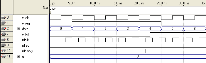
Figure 35. Functional Timing for the rdreq Signal and the rdempty SignalThis shows the behavior for the rdreq the rdempty signals.
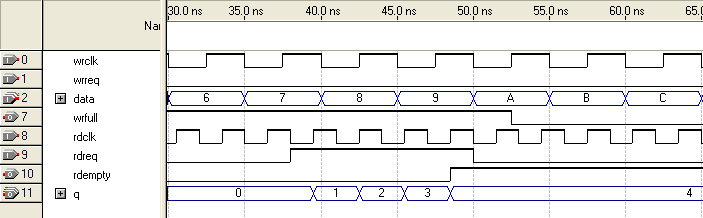
The required functional timing for the DCFIFO as described previously is also applied to the SCFIFO. The difference between the two modes is that for the SCFIFO, the wrreq signal must meet the functional timing requirement based on the full signal and the rdreq signal must meet the functional timing requirement based on the empty signal.