A newer version of this document is available. Customers should click here to go to the newest version.
4.3.13. Design Example
To obtain the DCFIFO settings in this design example, refer to the parameter settings from the design file (dcfifo8x32.v).
The following sections include separate simulation waveforms to describe how the write and read control logics generate the control signal with respect to the signal received from the DCFIFO.
- Signal values in binary format: reset, trclk, fifo_wrreq, fifo_wrfull
- Signal values in HEX format: rom_addr, rom_out, fifo_in
| State | Description |
|---|---|
| IDLE | Before reaching 10 ns, the reset signal is high and causes the write controller to be in the IDLE state. In the IDLE state, the write controller drives the fifo_wrreq signal to low, and requests the data to be read from rom_addr=00. The ROM is configured to have an unregistered output, so that the rom_out signal immediately shows the data from the rom_addr signal regardless of the reset. This shortens the latency because the rom_out signal is connected directly to the fifo_in signal, which is a registered input port in the DCFIFO. In this case, the data (0000000000000000000000000000000000000000000000000000000000000001) is always stable and pending to be written into the DCFIFO when the fifo_wrreq signal is high during the WRITE state. |
| WRITE | The write controller transitions from the IDLE state to the WRITE state if the fifo_wrfull signal is low after the reset signal is deasserted. In the WRITE state, the write controller drives the fifo_wrreq signal to high, and requests for write operation to the DCFIFO. The data is encoded through the embedded ECC block in the DCFIFO. The rom_addr signal is unchanged (00) so the data is stable for at least one clock cycle before the DCFIFO actually writes in the data at the next rising clock edge. |
| INCADR | The write controller transitions from the WRITE state to the INCADR state, if the rom_addr signal has not yet increased to ff (that is, the last data from the ROM has not been read out). In the INDADR state, the write controller drives the fifo_wrreq signal to low, and increases the rom_addr signal by 1 (00 to 01). |
| - | The same state transition continues as stated in IDLE and WRITE states, if the fifo_wrfull signal is low and the rom_addr signal not yet increased to ff. |
| State | Description |
|---|---|
| IDLE | Before reaching 35 ns, the read controller is in the IDLE state because the fifo_rdempty signal is high even when the reset signal is low (not shown in the waveform). In the IDLE state, the ram_addr = ff to accommodate the increment of the RAM address in the INCADR state, so that the first data read is stored at ram_addr = 00 in the WRITE state. |
| INCADR | The read controller transitions from the IDLE state to the INCADR state, if the fifo_rdempty signal is low. In the INCADR state, the read controller drives the fifo_rdreq signal to high, and requests for read operation from the DCFIFO. The data is decoded and the eccstatus shows the status of the data as no error detected (00), single-bit error detected and corrected(10), or uncorrectable error (11). The ram_addr signal is increased by one (ff to 00), so that the read data can be written into the RAM at ram_addr = 00. |
| WRITE | From the INCADR state, the read controller always transition to the WRITE state at the next rising clock edge. In the WRITE state, it drives the ram_wren signal to high, and enables the data writing into the RAM at ram_addr = 00. At the same time, the read controller drives the ram_rden signal to high so that the newly written data is output at q at the next rising clock edge. Also, it increases the word_count signal to 1 to indicate the number of words successfully read from the DCFIFO. |
| -- | The same state transition continues as stated in INCADR and WRITE states, if the fifo_rdempty signal is low. |
| State | Description |
|---|---|
| INCADR | When the write controller is in the INCADR state, and the fifo_wrfull signal is asserted, the write controller transitions to the WAIT state in the next rising clock edge. |
| WAIT | In the WAIT state, the write controller holds the rom_addr signal (08) so that the respective data is written into the DCFIFO when the write controller transitions to the WRITE state. The write controller stays in WAIT state if the fifo_wrfull signal is still high. When the fifo_wrfull is low, the write controller always transitions from the WAIT state to the WRITE state at the next rising clock edge. |
| WRITE | In the WRITE state, then only the write controller drives the fifo_wrreq signal to high, and requests for write operation to write the data from the previously held address (08) into the DCFIFO. It always transitions to the INCADR state in the next rising clock edge, if the rom_addr signal has not yet increased to ff. |
| -- | The same state transition continues as stated in INCADR, WAIT, and WRITE states, if the fifo_wrfull signal is high. |
| State | Description |
|---|---|
| WRITE | When the write controller is in the WRITE state, and rom_addr = ff, the write controller drives the fifo_wrreq signal to high to request for last write operation to DCFIFO. The data 100 is the last data stored in the ROM to be written into the DCFIFO. In the next rising clock edge, the write controller transitions to the DONE state. |
| DONE | In the DONE state, the write controller drives the fifo_wrreq signal to low. |
| -- | The fifo_wrfull signal is deasserted because the read controller in the receiving domain continuously performs the read operation. However, the fifo_wrfull signal is only deasserted sometime after the read request from the receiving domain. This is due to the latency in the DCFIFO (rdreq signal to wrfull signal). |
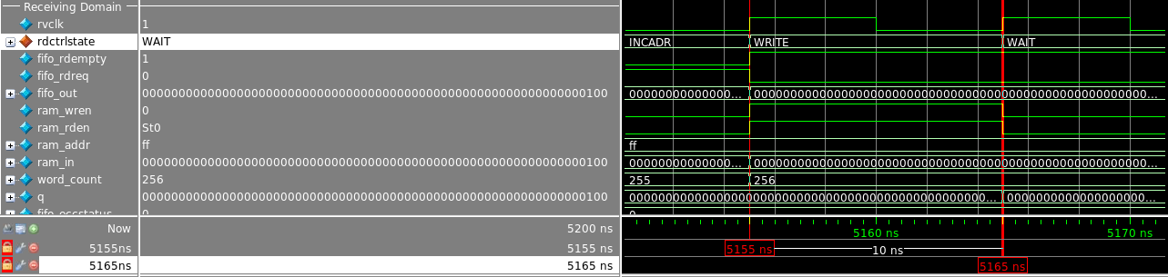
The fifo_rdempty signal is asserted to indicate that the DCFIFO is empty. The read controller drives the fifo_rdreq signal to low, and enables the write of the last data 100 at ram_addr =ff. The word_count signal is increased to 256 (in decimal) to indicate that all the 256 words of data from the ROM are successfully transferred to the RAM.
The last data written into the RAM is shown at the q output.