Intel® Quartus® Prime Pro Edition User Guide: Design Constraints
A newer version of this document is available. Customers should click here to go to the newest version.
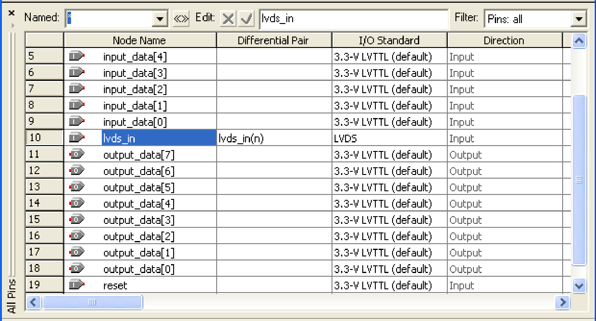
4.2.3. Assigning Differential Pins
When you assign a differential I/O standard to a single-ended top-level pin in your design, the Pin Planner automatically recognizes the negative pin as part of the differential pin pair assignment and creates the negative pin for you. The Intel® Quartus® Prime software writes the location assignment for the negative pin to the .qsf; however, the I/O standard assignment is not added to the .qsf for the negative pin of the differential pair.
The following example shows a design with lvds_in top-level pin, to which you assign a differential I/O standard. The Pin Planner automatically creates the differential pin, lvds_in(n) to complete the differential pin pair.
If your design contains a large bus that exceeds the pins available in a particular I/O bank, you can use edge location assignments to place the bus. Edge location assignments improve the circuit board routing ability of large buses, because they are close together near an edge. The following figure shows Intel device package edges.
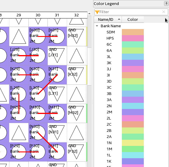
When you assign differential pin pairs in Package View, a red connection line displays between the pair of differential pins. The Package View labels the positive and negative pins with the letters p and n, respectively.