Developer Guide
Intel oneAPI DPC++/C++ Compiler Handbook for Intel FPGAs
A newer version of this document is available. Customers should click here to go to the newest version.
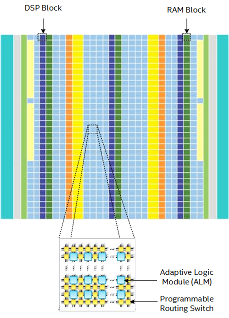
FPGA Architecture Overview
A field-programmable gate array (FPGA) is a reconfigurable semiconductor integrated circuit (IC).
FPGAs occupy a unique computational niche relative to other computing devices, such as central and graphics processing units (CPUs and GPUs), and custom accelerators, such as application-specific integrated circuits (ASICs). CPUs and GPUs have a fixed hardware structure to which a program maps. Conversely, ASICs and FPGAs can build custom hardware to implement a program.
While a custom ASIC generally outperforms an FPGA on a specific task, they take significant time and money to develop. However, FPGAs are a cheaper off-the-shelf alternative that you can reprogram for each new application.
An FPGA is made up of a grid of programmable logic blocks, which are called adaptive logic modules (ALMs) in FPGA devices, and specialized blocks, such as digital signal processing (DSP) blocks and random-access memory (RAM) blocks. These programmable blocks are connected via configurable routing interconnects to implement complete digital circuits.
The total number of ALMs, DSP blocks, and RAM blocks used by a design is often referred to as the FPGA area or area that the design uses.
The following image illustrates a high-level architectural view of an FPGA:
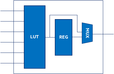
Adaptive Logic Module (ALM)
The basic building block in an FPGA is an adaptive logic module (ALM).
A simplified ALM consists of a lookup table (LUT) and an output register from which the compiler can build any arbitrary Boolean logic circuit.
The following figure illustrates a simplified ALM:
Lookup Table (LUT)
A lookup table (LUT) that implements an arbitrary Boolean function of N inputs is often referred to as an N-LUT.
Register
A register is the most basic storage element in an FPGA. It has an input (in), an output (out), and a clock signal (clk). It is synchronous, that is, it synchronizes output changes to a clock. In an ALM, a register may store the output of the LUT.
The following figure illustrates a register:
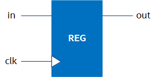
The clock signal is implied and not shown in some figures.
The following figure illustrates the waveform of register signals:
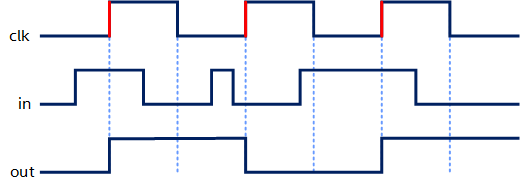
The input data propagates to the output on every clock cycle. The output remains unchanged between clock cycles.
Digital Signal Processing (DSP) Block
A digital signal processing (DSP) block implements specific arithmetic operations (addition and multiplication) that reduce the need to build equivalent logic from general-purpose ALMs. Some FPGAs support floating-point arithmetic in DSP blocks in addition to integer/fixed-point arithmetic. For more information, refer to Digital Signal Processing.
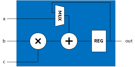
The following figure illustrates a simplified three-input DSP block consisting of a multiplier (×) and an adder (+):
Random Access Memory (RAM) Blocks
A random access memory (RAM) block provides more efficient storage of data than registers, making it suitable for collections of data that need not be accessed all at the same time. RAM blocks may either be implemented with dedicated block RAM modules (sometimes called M10K or M20K modules) or with specially configured ALMs called Memory-Logic Array Blocks (MLAB)s.
For more information, refer to Memory Types.