5.1. Package Heat Flow Path
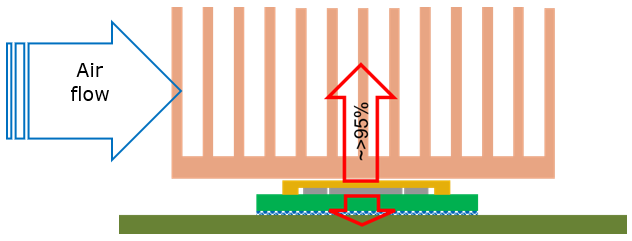
The ΨCA output from the PTC determines how large or efficient the heat sink on the package needs to be. Currently, it is calculated considering all heat generated by the FPGA goes out through the top of the package (through the lid in a lidded package and through the die in a lidless package). These are true for high power packages which have high performance heat sinks on top and generally include forced air flow over the heat sink. The following figure reperesents this condition:
Usually, in systems with low power FPGAs (<5W), the packages might have small (low performance) heat sinks, commonly without any additional airflow. In such cases, only a fraction of the heat generated in the die flows through the top of the package into the heat sink. The remaining heat flows through the substrate of the package and into the PCB. The fraction of heat through to the PCB depends on system design and other boundary conditions. The following figure illustrates this case.

For these system conditions, due to lack of sufficient airflow and/or available space, it is not possible to increase the heat sink performance significantly. In such a scenario, to avoid designing unnecessarily large heat sinks, it is important to size the heat sink while taking into consideration only the amount of heat dissipated through the top of the die and not the amount of heat that can be dissipated through the PCB.
The fraction of heat dissipated through the substrate into the PCB depends on various factors, including:
- Local ambient temperature inside the system.
- Air flow above and below the PCB.
- Heat sink type, material, size, clamping load.
- Thermal interface material (TIM) between the FPGA and heat sink – TIM material and thickness.
- Shared heat sink contacting other components that potentially have larger heat loss or higher temperatures.
- Other high power and high temperature components on the PCB and close to the FPGA that might affect the local PCB temperature.
- PCB construction, such as the number of layers, copper density in the layers, etc.
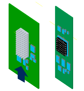
The following figure illustrates differences in board layout, thermal solution sizes and flow condition.
Considering the factors discussed above, it has been seen in a small set of systems that the fraction of heat generated in the device dissipating through the top of the device — and if applicable, to the heat sink — ranges between 10% and 90%. Because this is a large range, it is essential that the heat sink be optimally sized to handle the actual amount of heat passing through the top of the device.