AN 1000: Drive-on-Chip Design Example: Agilex™ 5 Devices
ID
826207
Date
7/08/2024
Public
1. About the Drive-on-Chip Design Example for Agilex™ 5 Devices
2. Features of the Drive-on-Chip Design Example for Agilex Devices
3. Getting Started with the Drive-on-Chip Design Example
4. Rebuilding the Drive-on-Chip Design Example
5. Modifying the Design Example for a Different Board
6. About the Scaling of Feedback Signals
7. Motor Control Software
8. Functional Description of the Drive-on-Chip Design Example for Agilex 5 Devices
9. Signals
10. Registers
11. Design Security Recommendations
12. Document Revision History for AN 1000: Drive-on-Chip Design Example for Agilex™ 5 Devices
3.1. Software Requirements for the Drive-on-Chip Design Example for Agilex 5 Devices
3.2. Hardware Requirements for the Drive-on-Chip Design Example for Agilex 5 Devices
3.3. Downloading and Installing the Design
3.4. Setting Up your Development Board for the Drive-on-Chip Design Example for Agilex 5 Devices
3.5. Configuring the FPGA Hardware for the Drive-on-Chip Design Example for Agilex 5 Devices
3.6. Programming the Nios V/g Software to the Device for the Drive-on-Chip Design Example for Agilex Devices
3.7. Debugging and Monitoring the Drive-on-Chip Design Example for Agilex 5 Devices with Python GUI
8.3.6.1. DSP Builder Model for the Drive-on-Chip Designs
8.3.6.2. Avalon Memory-Mapped Interface
8.3.6.3. About DSP Builder for Intel FPGAs
8.3.6.4. DSP Builder for Intel FPGAs Folding
8.3.6.5. DSP Builder for Intel FPGAs Design Guidelines
8.3.6.6. Generating VHDL for the DSP Builder Models for the Drive-on-Chip Designs
5. Modifying the Design Example for a Different Board
Altera provides the design for the Agilex™ 5 FPGA E-Series 065B Modular Development Kit. To target the design to a different Agilex 5 development board, follow these steps:
- Find the part number of your board. The original design is for A5ED065BB32AE6SR0.
- Navigate to Assignments > Assignment Editor.
Figure 15. Assignment Editor
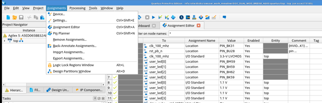
- Modify the location of the main clock, in the original design with the name of clk_100_mhz (but it can be other rate) and the reset push button rst_pb_n. The reset button is originally active low.
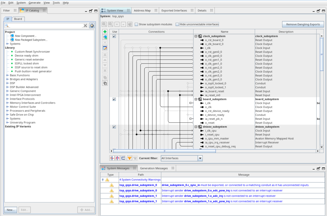
- Only if the rate of the clock is different than 100 MHz, open Platform Designer, navigate to Tools > Platform Designer”
- In the new window, open the file top_qsys.qsys by clicking (…) in the Platform Designer system drop down menu. Click Select and then Open.
You should see the top-level Platform Designer Project in the <project>/rtl directory.Figure 16. Top-level Platform Designer Project
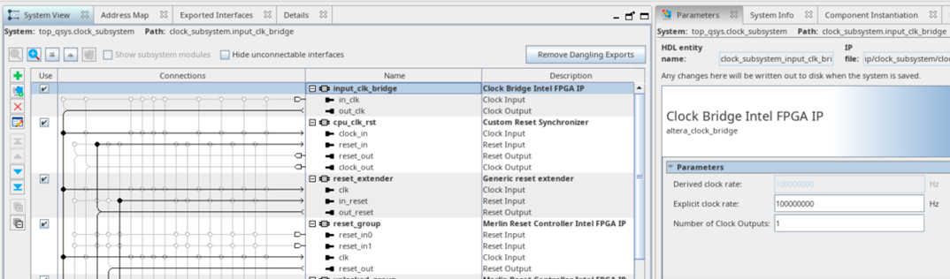
- To verify the clock rates, select the clock subsystem and click Drill into subsystem to explore its contents
- Click the input_clk_bridge block and set the Explicit clock rate according to your board clock rate pin in Hz
Figure 17. input_clk_bridge Block
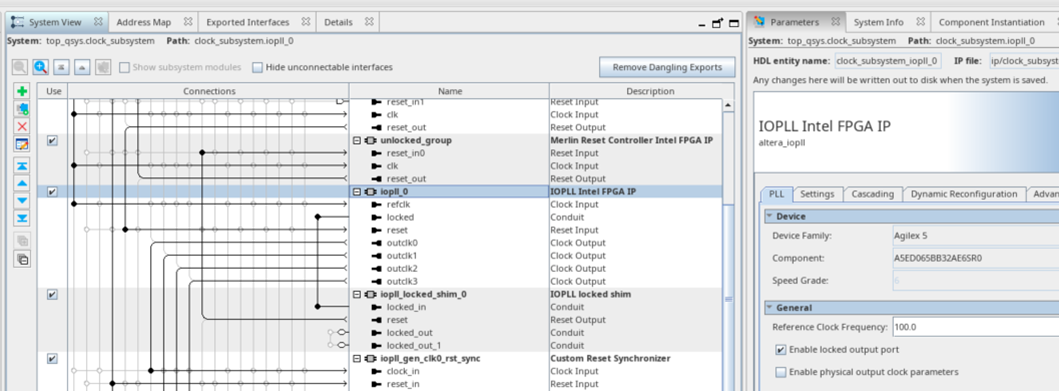
- Select the iopll_0 block and modify the Reference Clock Frequency option.
Figure 18. iopll_0 Clock
- Click Generate HDL…. When it finishes, close Platform Designer.
- Recompile your design in Quartus Prime Pro.