GTS AXI Streaming IP for PCI Express* Design Example User Guide
1.3.1. Single-Root I/O Virtualization (SR-IOV) Design Example Functional Description
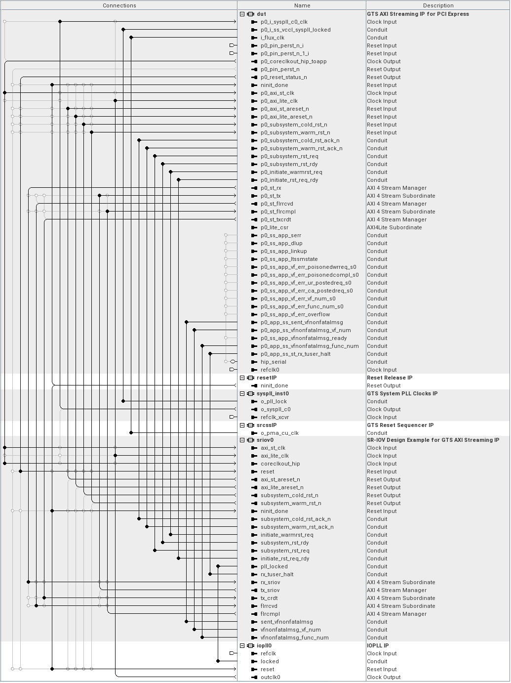
- The DUT component is the GTS AXI Streaming IP for PCI Express configured as an Endpoint interacting with the root complex/switch on one end, and drives the received TLP data to the SR-IOV application at the other end. The DUT component translates the PCIe serial link transfer interface to the AXI Stream interface.
- The SR-IOV Design Example for GTS AXI Streaming IP component interfaces with the DUT through the AXI Stream interface. It initiates a series of RAMs to store the incoming data from the DUT. The number of RAM is determined by PF and VF from the user. During operation modes, the SR-IOV Design Example for GTS AXI Streaming IP decodes the TLP headers/data into Memory write or Memory read instructions. If the instructions are valid, Memory write or Memory read is performed to the PF and VF Segram according to the PF and VF information from the AXI Stream interface with DUT, which performs the necessary translation between the PCI Express TLPs and simple AXI Stream writes and reads to the on-chip memory.
- Access Parser
Access Parser is a submodule to decode and validate the incoming instruction, whether it is valid and good to proceed to the next phase of processing. It ensures the target address and data are double-word aligned. If the received Memory write instruction does not fulfill the requirement, it is silently dropped. While for Memory read instruction, which does not fulfill the requirement, it will be a Completer Abort.
- Access Router
Access Router is a network of connections that connects all the instantiated Segrams. It reroutes the data from the source to the target destination. Based on the decoded PF and VF information from the Access Parser, the targeted Segram activates, and does further processing.
- Completion
The Completion submodule stores the necessary header information from the incoming Memory read instruction and repackages the acquired information into a CplD header. The CplD header is released together with the fetched data from the targeted Segram.
- PF Segram
The PF Segram is a RAM instantiated from the design example based on the PF number. Each RAM instantiated consists of 64-bit data width and is 64 deep, for a total of 4 KB.
- VF Segram
The VF Segram is a RAM instantiated from the SR-IOV Design Example based on the PF and VF number. Each RAM instantiated consists of a 64-bit data width and is 64 deep, for a total of 4 KB.
- Access Parser
- Transmit Flow Control
Note: Refer to Transmit Flow Control for additional information.
- Soft Reset Controller
Note: Refer to Soft Reset Controller for additional information.
- AXI-S to Avalon-ST Adapter
Note: Refer to AXI-S to Avalon-ST Adapter for additional information.
- GTS System PLL Clocks IP
Note: Refer to GTS System PLL Clocks IP for additional information.
- GTS Reset Sequencer IP
Note: Refer to GTS Reset Sequencer IP for additional information.
- Reset Release IP
Note: Refer to Reset Release IP for additional information.