GTS AXI Streaming IP for PCI Express* Design Example User Guide
ID
817713
Date
10/23/2025
Public
2.1. Directory Structure
2.2. Generating the Design Example
2.3. Simulating the Design Example
2.4. Design Example Simulation Testbench
2.5. Compiling the Design Example
2.6. Hardware and Software Requirements
2.7. Program the FPGA
2.8. Installing the Linux Kernel Driver
2.9. Running the Design Example
A.1.1. ebfm_barwr Procedure
A.1.2. ebfm_barwr_imm Procedure
A.1.3. ebfm_barrd_wait Procedure
A.1.4. ebfm_barrd_nowt Procedure
A.1.5. ebfm_cfgwr_imm_wait Procedure
A.1.6. ebfm_cfgwr_imm_nowt Procedure
A.1.7. ebfm_cfgrd_wait Procedure
A.1.8. ebfm_cfgrd_nowt Procedure
A.1.9. BFM Configuration Procedures
A.1.10. BFM Shared Memory Access Procedures
A.1.11. BFM Log and Message Procedures
A.1.12. Verilog HDL Formatting Functions
2.2. Generating the Design Example
Figure 11. Procedure to Generate Design Example
- In the Quartus® Prime Pro Edition software, create a new project (File ➤ New Project Wizard). Click Next.
- Select Empty project type and specify the Directory, Name and Top-Level Entity. Click Next.
- For Family, Device & Board Settings under Family, select Agilex 3 or Agilex 5, and then select Target Device for your design. After that, click Finish to proceed.
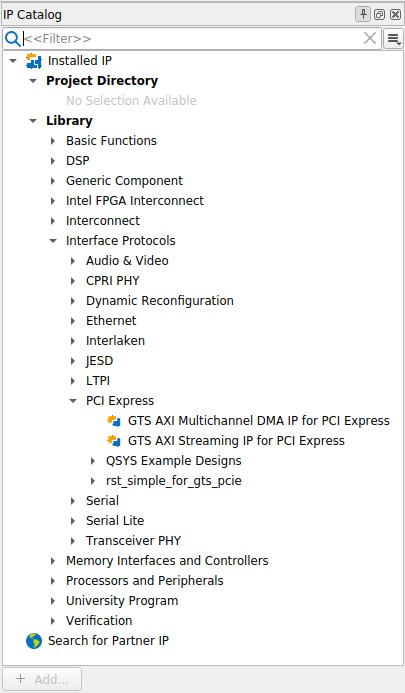
- Select Tools → IP Catalog to open the IP Catalog. Then, select GTS AXI Streaming IP for PCI Express (Library → Interface Protocols → PCI Express → GTS AXI Streaming IP for PCI Express), and then click Add.
- In the New IP Variant dialogue box, specify a top-level name for your new custom IP variant and the directory for it. The IP Parameter Editor saves the IP variant settings in a file named <your_ip>.ip.
- Click Create. The GTS AXI Streaming IP for PCI Express IP Parameter Editor displays IP Settings, PCIe Settings, and Example Designs tabs to allow you to quickly configure your custom IP variant.
- On the System Settings tabs, specify the parameters for your IP variation.
- On the Example Designs tab, make the following selections:
- For Example Design Files, turn on the Simulation and Synthesis options. If you do not need these simulation or synthesis files, leaving the corresponding option(s) turned off significantly reduces the design example generation time.
- For Generated HDL Format, only Verilog is supported in the current release.
- For Currently Selected Example Design, the PIO, SRIOV, and Performance design examples are supported in this release.
- For Target Development Kit, select either the Agilex™ 5 FPGA E-Series 065B Modular Development Kit (ES1) (for the Agilex™ 5 device family only) or NONE to target the device selected for your current Quartus® Prime software project. When the Agilex™ 3 device is selected for the project, the Agilex™ 3 FPGA C-Series 135B Non-HPS Development Kit (Production) and NONE options are available instead. If you select the development kit, the settings including the pin assignments are included in the .qsf file of the generated design example, and you are not required to add them manually. These settings are board-specific for the development kit.
Figure 12. Example Designs Tab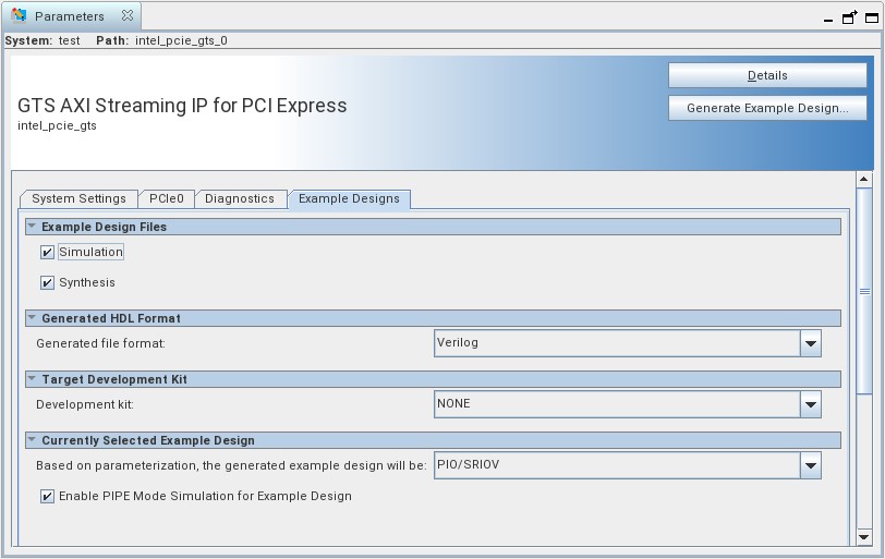
- Click Generate Example Design to generate the design example variant. When the prompt asks you to specify the directory for your design example, you can accept the default directory, /pcie_gts_0_example_design, or choose another directory. Then, click OK to kick off the design example generation.
- Click Finish. You may save your .ip file when prompted, but it is not required to be able to use the design example.