A newer version of this document is available. Customers should click here to go to the newest version.
4.7.2.1.1. Hardware Design Flow
The following sections describe a step-by-step method for building a bootable system for a Nios® V processor application copied from configuration QSPI flash to RAM using Bootloader via GSFI. The following example is built using Arria® 10 SoC Development Kit.
IP Component Settings
- Create your Nios® V processor project using Quartus® Prime and Platform Designer.
- Add the Generic Serial Flash Interface Altera® FPGA IP is into your Platform Designer system.
Figure 114. Connections for Nios® V Processor ProjectFigure 115. Generic Serial Flash Interface Altera® FPGA IP Parameter Settings
- Change the Device Density (Mb) according to the QSPI flash size.
- Change the addressing mode by modifying bit 8 of the Control Register value in the Default Settings parameter section. Changing bit 8 to 0x0 enables 3-byte addressing, or 0x1 enables 4-byte addressing
For example, Arria® 10 devices when used with Micron flash devices support the 4-byte addressing mode.
Reset Agent Settings for Nios® V Processor Boot-copier Method
- In the Nios® V processor parameter editor, set the Reset Agent to QSPI Flash.
Note: Your SOF image size influences your reset offset configuration. The reset offset is the start of the address of the HEX file in QSPI flash and it must point to a location after the SOF image. If the SOF image space and the reset offset location overlap, Quartus® Prime software displays and overlap error. You can determine the minimum reset offset by using the configuration bitstream size from the device datasheet.
For example, the uncompressed configuration bitstream size for Arria® 10 GX 660 is 252,959,072 bits (31,619,884 bytes). If the SOF image starts at address 0x0, the SOF image can extend up to address 0x1E27FFF (0x1E27B2C). In this case, the minimum reset offset you can select is 0x2000000.
Figure 116. Nios V Parameter Editor Settings - Click Generate HDL, the Generation dialog box appears.
- Specify output file generation options and then click Generate.
Quartus® Prime Software Settings
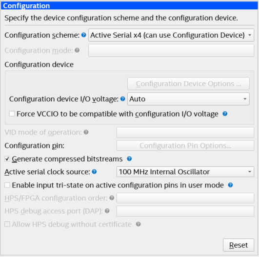
- In the Intel Quartus Prime software, click Assignment > Device > Device and Pin Options > Configuration .
- Set Configuration scheme to Active Serial x4 (can use Configuration Device).
- Set the Active serial clock source to 100 MHz Internal Oscillator.
Figure 117. Device and Pin Options
- Click OK to exit the Device and Pin Options window.
- Click OK to exit the Device window.
- Click Start Compilation to compile your project.