Agilex™ 7 FPGA I-Series Transceiver-SoC Development Kit User Guide
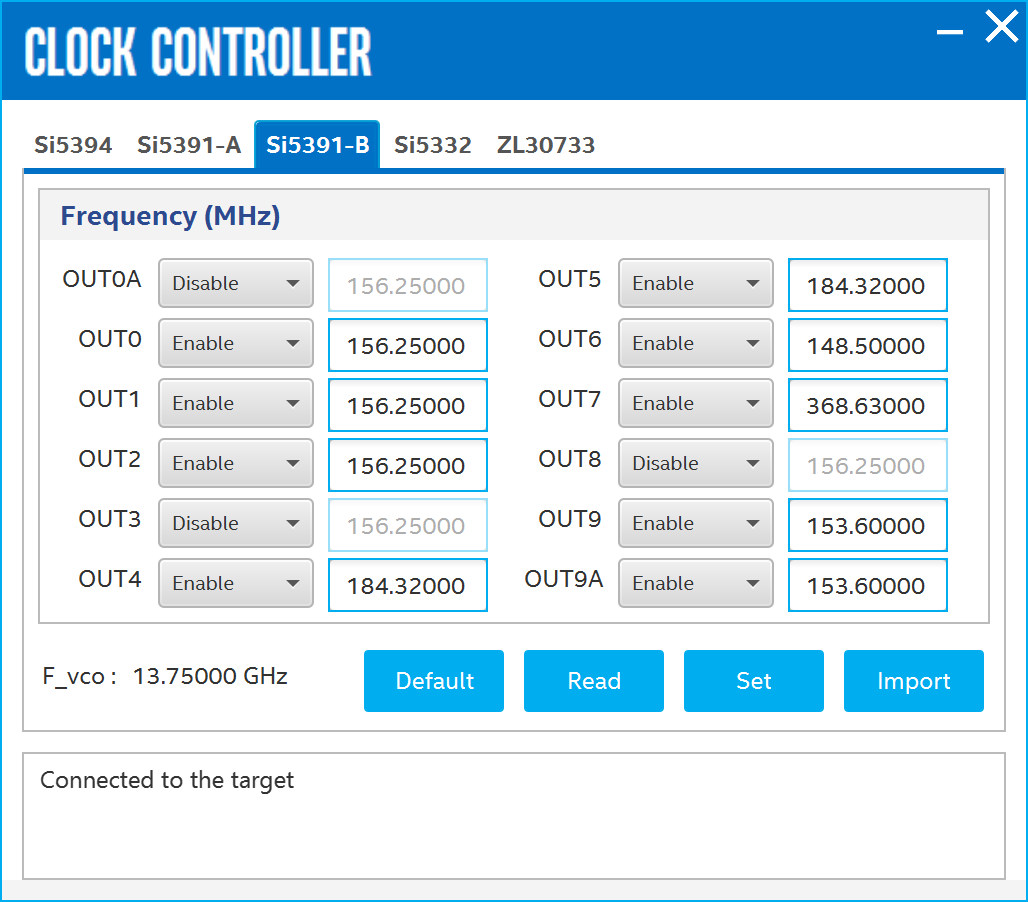
4.3. Control On-Board Clock through Clock Controller GUI
The Clock Controller communicates with the system MAX® 10/ Agilex™ 7 device through a 10-pin JTAG header J11 or USB port J10. The system MAX® 10 controls Si5394/Si5391-A/Si5391-B/Si5332, and Agilex™ 7 device controls ZL30733 through the I2C bus.
The instructions to run the Clock Controller GUI are stated in the Running the BTS GUI section. Alternatively, you can start using the Clock Controller feature by selecting the Clock icon on the BTS GUI.
The following sections describe the Clock Controller GUI buttons.
Read
Reads the current frequency setting for the oscillator associated with the active tab.
Default
Sets the frequency for the oscillator associated with the active tab back to its default value. This can also be accomplished by power cycling the board.
Set
Sets the programmable oscillator frequency for the selected clock to the value in the OUTx output controls for Si5394. Frequency changes might take several milliseconds to take effect. You might see glitches on the clock during this time. Altera recommends resetting the FPGA logic after changing frequencies.
Import
Si5394 has a two-time rewritable non-volatile memory (NVM). You can generate the register list from the Clockbuilder Pro tool and import it into Si5394 to update the settings of the RAM. Register changes are volatile after power cycling.
The output frequency of ZL30733 is from 0.5 Hz to 750 MHz. It can generate up to 10 differential outputs with a total of 5 output frequency families.
Import
- Register Write Command Link: X,<register_address>, <data_bytes>, <register_address> and <data_bytes>, where prefix must be "0x" are in hexadecimal
- Wait Command Line: W, <time_microseconds>
Import it into ZL30733 to update the RAM settings. Register changes are volatile after power cycling. For more details, refer to ZL30733 on the Microchip website.