1.4. Generating the Design Example
Figure 5. Procedure
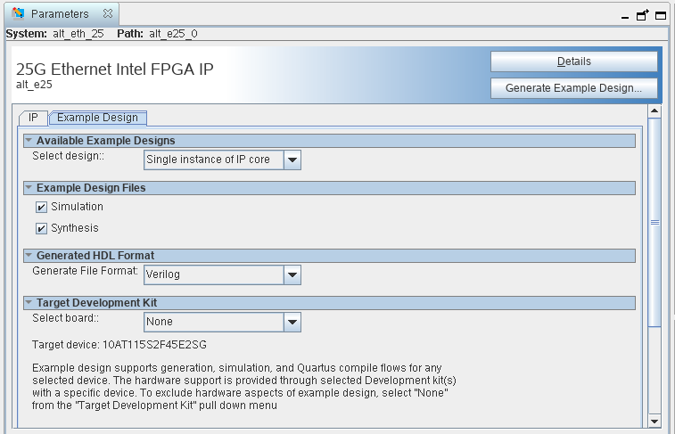
Figure 6. Example Design Tab in the 25G Ethernet Intel FPGA IP Parameter Editor
Follow these steps to generate the hardware design example and testbench:
- Depending on whether you are using the Intel® Quartus® Prime Pro Edition software or the Intel® Quartus® Prime Standard Edition software, perform one of the following actions:
- In the Intel® Quartus® Prime Pro Edition, click to create a new Quartus Prime project, or to open an existing Quartus Prime project. The wizard prompts you to specify a device.
- In the Intel® Quartus® Prime Standard Edition software, in the IP Catalog (), select the Intel® Arria® 10 target device family.
- In the IP Catalog, locate and select 25G Ethernet. The New IP Variation window appears.
- Specify a top-level name for your IP variation and click OK. The parameter editor adds the top-level .qsys (in Intel® Quartus® Prime Standard Edition) or .ip (in Intel® Quartus® Prime Pro Edition) file to the current project automatically. If you are prompted to manually add the .qsys or .ip file to the project, click to add the file.
- In the Intel® Quartus® Prime Standard Edition software, you must select a specific Intel® Arria® 10 device in the Device field, or keep the default device the Quartus Prime software proposes.
- Click OK. The parameter editor appears.
- On the IP tab, specify the parameters for your IP core variation.
- On the Example Design tab, for Example Design Files, select the Simulation option to generate the testbench, and select the Synthesis option to generate the hardware design example. Only Verilog HDL files are generated.
Note: A functional VHDL IP core is not available. Specify Verilog HDL only, for your IP core design example.
- Click the Generate Example Design button. The Select Example Design Directory window appears.
- If you wish to modify the design example directory path or name from the defaults displayed (alt_e25_0_example_design ), browse to the new path and type the new design example directory name (<design_example_dir>).
- Click OK.
- Refer to the KDB Answer How do I compensate for the jitter of PLL cascading or non-dedicated clock path for Arria 10 PLL reference clock? for a workaround you should apply in the hardware_test_design directory in the .sdc file.
Note: You must consult this KDB Answer because the RX path in the 25G Ethernet Intel FPGA IP core includes cascaded PLLs. Therefore, the IP core clocks might experience additional jitter in Intel® Arria® 10 devices. This KDB Answer clarifies the software releases in which the workaround is necessary.